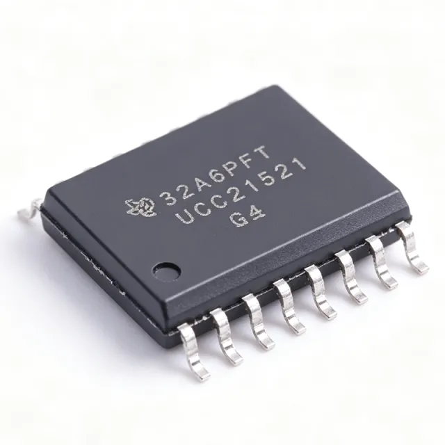
UCC21521DWR - 4A/6A 5.7kVrms Isolated Gate Driver | TI
MPN: UCC21521DWR ✓ Active| Qty | Unit Price | Extended |
|---|---|---|
| 1 | $4.2 | $4.20 |
| 10 | $3.78 | $37.80 |
| 100 | $3.3 | $330.00 |
| 500 | $2.92 | $1,460.00 |
| 1,000 | $2.65 | $2,650.00 |
UCC21521DWR Overview
An isolated gate driver is a power-management IC that translates low-voltage control logic from a microcontroller or DSP into the high peak current required to switch power transistors, while maintaining galvanic isolation between the control side and the power stage. Within the power-electronics hierarchy it sits between PWM controllers and MOSFETs, IGBTs, or SiC MOSFETs, and it is essential for safety isolation and noise immunity in high-voltage converters.
Key features include 19-ns typical propagation delay, 5-ns maximum channel-to-channel matching, 6-ns maximum pulse-width distortion, and a 10-ns minimum input pulse width. These tight timing specifications reduce switching losses and minimize shoot-through risk. The DIS enable pin supports power sequencing and fast fault shutdown, and programmable dead time (for half-bridge configurations) prevents cross-conduction.
Technically, the UCC21521 uses TI capacitive isolation technology to deliver the 5.7-kV RMS reinforced barrier with CMTI of at least 100 V/ns, making it robust in high dv/dt SiC environments. Input thresholds are TTL and CMOS compatible for direct 3.3-V logic interfacing, and an 8-V UVLO protects the power switch from under-driven operation.
Typical applications include motor drives, solar string inverters, EV onboard chargers, and isolated DC-DC converters, where the 4-A/6-A drive strength and up-to-5-MHz switching capability suit SiC and IGBT power stages.
Design tip: place decoupling capacitors directly at VCCI and VDDA/VDDB pins and minimize gate-loop inductance to achieve the datasheet timing figures and avoid dv/dt-induced false triggering.
This page adds value beyond the datasheet with drop-in alternative comparisons, pricing tiers, and practical layout notes synthesized from distributor and manufacturer data.
Drop-in alternatives for UCC21521DWR — same package, pin-to-pin compatible. Different-package parts requiring PCB rework are excluded.
Variants in this series
Same-series models that are drop-in compatible with UCC21521DWR (same form factor and footprint) — differing in Package, Isolation Rating, Isolation Technology, Enable Pin, Isolation Type.
Quick Comparison Tool — Select alternative parts for side-by-side comparison:
UCC21521ADWR
✅ Drop-In✓ In Stock
$2.41 / Unit
View Datasheet →UCC21521Q-Q1
✅ Drop-In✓ In Stock
$1 / Unit
View Datasheet →UCC21521DWR
✅ Drop-In✓ In Stock
$2.15 / Unit
View Datasheet →UCC21540
✅ Drop-In ⚠️ Specs Unverified✓ In Stock
$1.85 / Unit
View Datasheet →UCC21520
✅ Drop-In ⚠️ Specs Unverified✓ In Stock
$1.55 / Unit
View Datasheet →UCC21550BDWR
✅ Drop-In ⚠️ Specs Unverified✓ In Stock
$0.88 / Unit
View Datasheet →UCC21521DWR Maximum Ratings & Electrical Characteristics
| Number of Channels | 2 |
| Peak Output Source Current | 4 A |
| Peak Output Sink Current | 6 A |
| Isolation Rating | 5700 Vrms (reinforced) |
| Common-Mode Transient Immunity (CMTI) | >= 100 V/ns |
| Propagation Delay (typical) | 19 ns |
| Channel Matching (max) | 5 ns |
| Pulse-Width Distortion (max) | 6 ns |
| Minimum Input Pulse Width | 10 ns |
| Output Supply UVLO | 8 V |
| Switching Frequency (max) | 5 MHz |
| Driver Configuration | Dual low-side / dual high-side / half-bridge (universal) |
| Enable Pin | Yes (DIS, disable) |
| Input Threshold Compatibility | TTL / CMOS compatible (3.3 V logic) |
| Operating Temperature | -40C to +125C |
| Package | 16-pin SOIC (DW) |
| Mounting Type | Surface Mount |
| Isolation Technology | Capacitive isolation |
UCC21521DWR Pin Configuration
| Pin 1 | VCCI — 3.3-V to 5-V input-side supply |
| Pin 2 | GND — Input-side ground reference |
| Pin 3 | DIS — Disable input (enable/disable pin) |
| Pin 4 | IN_A — Input signal, channel A |
| Pin 5 | IN_B — Input signal, channel B |
| Pin 6 | NC — Not connected (per datasheet) |
| Pin 7 | NC — Not connected (per datasheet) |
| Pin 8 | NC — Not connected (per datasheet) |
| Pin 9 | NC — Not connected (per datasheet) |
| Pin 10 | NC — Not connected (per datasheet) |
| Pin 11 | VDDA — Output driver A supply |
| Pin 12 | OUTA — Gate drive output, channel A |
| Pin 13 | GNDA — Output-side ground reference A |
| Pin 14 | GNDB — Output-side ground reference B |
| Pin 15 | OUTB — Gate drive output, channel B |
| Pin 16 | VDDB — Output driver B supply |
Typical Applications
UCC21521DWR is suitable for 6 applications: Three-Phase Motor Drives, Solar String Inverters, EV Onboard Chargers and OBC/DC-DC, Isolated DC-DC Converters, SiC MOSFET Power Modules, Industrial Power Supplies and Welders.
Three-Phase Motor Drives
In industrial three-phase inverters, each leg of the power stage requires an isolated half-bridge gate driver, and the UCC21521DWR fits this role with 4-A source / 6-A sink peak current that quickly charges and discharges IGBT or SiC MOSFET gate capacitances, reducing switching losses. The 5.7-kV RMS reinforced barrier isolates the low-voltage MCU from the high-voltage DC bus for safety compliance, while CMTI of at least 100 V/ns keeps the driver immune to the large dv/dt at the switching node. Its programmable dead time prevents shoot-through between high- and low-side switches, and the DIS enable pin allows instant shutdown on fault detection from the motor-control DSP. Positioned between a 3.3-V PWM controller and the gate networks, it delivers the timing precision (5-ns matching) needed for balanced phase currents.
Recommended
Solar String Inverters
Grid-tied solar string inverters combine a boost stage and a DC-AC bridge where the UCC21521DWR provides isolated gate drive for the high-side and low-side power switches. The 5.7-kV RMS reinforced isolation supports the system-level insulation requirements between PV input, AC grid, and control electronics. Its 19-ns propagation delay and 100 V/ns CMTI are well matched to SiC MOSFET switching in the 20-100 kHz range, where high dv/dt on the switching node would falsely trigger weaker isolation technologies. The 8-V UVLO ensures the SiC devices are never driven below their minimum recommended gate voltage, preventing operation in a high-Rds(on) regime that causes thermal runaway. The enable pin lets the inverter controller gate off all bridges within nanoseconds during grid faults or MPPT transients.
Recommended
EV Onboard Chargers and OBC/DC-DC
Electric-vehicle onboard chargers use PFC plus isolated LLC stages that switch at high frequency, and the UCC21521DWR supports this with operation up to 5 MHz and a 10-ns minimum pulse width, enabling compact high-frequency magnetics. The 4-A/6-A drive strength handles the large gate charge of SiC MOSFETs typical in 6.6-kW to 22-kW OBC designs, while the 5.7-kV RMS barrier satisfies isolation between the traction battery and AC mains. The -40C to +125C operating range covers under-hood and near-battery thermal environments. Its tight 5-ns channel matching keeps LLC bridges symmetric, minimizing transformer flux imbalance. For automotive-qualified builds, the UCC21521Q-Q1 variant adds AEC-Q100 compliance without PCB changes.
Recommended
Isolated DC-DC Converters
Telecom and industrial isolated DC-DC converters (half-bridge and full-bridge LLC topologies) use the UCC21521DWR to drive primary-side power switches with galvanic isolation from the control loop. The 19-ns typical propagation delay and 6-ns maximum pulse-width distortion preserve duty-cycle accuracy at the 100 kHz-1 MHz switching frequencies these converters use, directly reducing output ripple and improving transient response. The 100 V/ns CMTI is essential in LLC bridges where the midpoint slews rapidly every cycle. With the DIS pin, a supervisory circuit can disable both outputs during start-up sequencing or overcurrent events. The dual-input architecture supports both dual low-side and half-bridge configurations, letting one driver IC serve multiple converter topologies across a product family.
Recommended
SiC MOSFET Power Modules
SiC-based power modules in traction inverters, energy storage converters, and high-power supplies demand gate drivers with high CMTI and strong sink current, and the UCC21521DWR delivers both: at least 100 V/ns common-mode transient immunity and a 6-A pull-down that holds SiC gates firmly low against Miller-induced turn-on. The 8-V UVLO is deliberately matched to SiC gate-drive levels, blocking operation until VDDA/VDDB is adequate. Its capacitive isolation technology maintains the 5.7-kV RMS reinforced rating across temperature and aging, supporting the functional-safety isolation of high-voltage stages. The universal input architecture lets the same component drive dual low-side switches in boost PFC or a high/low-side half-bridge in the inverter stage of the same system.
Recommended
Industrial Power Supplies and Welders
High-power industrial AC-DC supplies, welding inverters, and induction-heating converters rely on the UCC21521DWR for robust isolated gate drive in electrically noisy environments. The reinforced 5.7-kV RMS isolation separates operator-accessible controls from hazardous voltages, while the TTL/CMOS-compatible inputs connect directly to 3.3-V controllers without level shifting. Its 4-A/6-A peak currents switch large IGBT modules efficiently at the 20-50 kHz frequencies typical of welding inverters, and the 100 V/ns CMTI withstands the severe dv/dt generated by hard-switched current ramps. The enable pin provides a fast, deterministic shutdown path for the overcurrent and overtemperature protection loops required in these high-energy systems, complementing module-level desaturation protection.
Recommended
Recommended Products Summary
Engineering reference data for UCC21521DWR — comparison, design guidance, and compliance information.
Selection Guide
Comparison with Alternatives
| Parameter | This Product | UCC21521ADWR | UCC21521Q-Q1 | UCC21520 | UCC21540 | UCC21550BDWR |
|---|---|---|---|---|---|---|
| Package | 16-SOIC (DW) | 16-SOIC (DW) - same | 16-SOIC (DW) - same | 16-SOIC (DW) - same | 16-SOIC (DW) - same | 16-SOIC (DW) - same |
| Brand | Texas Instruments | Texas Instruments | Texas Instruments | Texas Instruments | Texas Instruments | Texas Instruments |
| Automotive Grade | No | No | Yes (AEC-Q100) | No | Q1 variant available | B-grade variant available |
Key Differentiators
- Enable (DIS) pin for fast fault shutdown (vs UCC21520)
- AEC-Q100 automotive option on the same footprint (vs UCC21521Q-Q1)
- 4-A source / 6-A sink asymmetric drive (vs UCC21520)
Design Notes
Place a 0.1-uF ceramic capacitor in parallel with a bulk capacitor directly across VCCI-GND, and identical pairs across VDDA-GNDA and VDDB-GNDB, within 2-3 mm of the pins. Because the two output grounds (GNDA/GNDB) are separate, route their returns individually back to their respective power-stage source terminals rather than tying them near the IC, which defeats the intended isolation. On a 4-layer board, use an uninterrupted ground plane on layer 2 and stitch the input-side ground region away from the output-side switching copper.
Minimize the gate loop: keep the OUTA/OUTB trace to the MOSFET gate and the return path via GNDA/GNDB as short and wide as possible; every nH of loop inductance causes gate ringing with a 4-A/6-A drive. Add a small external gate resistor (2-10 ohm typical) to damp ringing and control switching speed, and optionally a pull-down resistor (10 kohm) at each gate to hold SiC MOSFETs off while VDDA/VDDB is below the 8-V UVLO threshold during start-up.
Even with 100 V/ns CMTI, careless layout can couple dv/dt into input-side signals. Route the IN_A/IN_B and DIS traces away from the switching node and away from the isolation gap crossing; do not run control traces under or adjacent to OUTA/OUTB copper. Also note the DIS pin must be actively driven or biased to a defined level - leaving it floating can produce undefined enable states at power-up; a pull-up or pull-down resistor consistent with the required default state is best practice.
Estimated: gate-drive dissipation per channel is Qg x fsw x VDD; for example a SiC MOSFET with 60-nC gate charge at 100 kHz and 18-V drive dissipates about 0.11 W per channel in the driver plus resistor losses. The 16-SOIC (DW) package handles this without heatsinking, but verify junction temperature stays below +125C by accounting for driver quiescent power and layout copper area on VDDA/VDDB nets.
Compliance Information
Standard TI UCC21521 (DWR suffix) is RoHS-compliant and lead-free per TI product page. Automotive AEC-Q100 qualification applies to the UCC21521Q-Q1 variant, not this part number. REACH and halogen-free status not stated in provided data.







