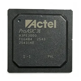
10CL080ZU484I8G - 81,264 Logic Elements FPGA | Intel | Embedded Systems
MPN: 10CL080ZU484I8G ✓ Active| Qty | Unit Price | Extended |
|---|---|---|
| 1 | $0 | $0.00 |
| 10 | $0 | $0.00 |
| 100 | $0 | $0.00 |
| 500 | $0 | $0.00 |
| 1,000 | $0 | $0.00 |
Drop-in alternatives for 10CL080ZU484I8G — same package, pin-to-pin compatible. Different-package parts requiring PCB rework are excluded.
Quick Comparison Tool — Select alternative parts for side-by-side comparison:
10CL080ZF484I8G
✅ Drop-In ⚠️ 参数待验证✓ In Stock
$64.5 / Unit
View Datasheet →10CL080YU484I7G
✅ Drop-In ⚠️ 参数待验证✓ In Stock
$152 / Unit
View Datasheet →10CL080YU484C8G
✅ Drop-In ⚠️ 参数待验证✓ In Stock
$450 / Unit
View Datasheet →10CL080YU484C6G
✅ Drop-In ⚠️ 参数待验证✓ In Stock
$34.75 / Unit
View Datasheet →10CL080YU484A7G
✅ Drop-In ⚠️ 参数待验证✓ In Stock
$171 / Unit
View Datasheet →10CL080ZU484I8G Maximum Ratings & Electrical Characteristics
| Product Type | Field Programmable Gate Array (FPGA) |
| Device Family | Cyclone 10 LP |
| Logic Elements | 81,264 |
| Embedded Memory | 2,810,880 bit |
| I/O Count | 289 |
| Package | 484-FBGA |
| Ordering Package Designation | U484 |
| Pin Count | 484 |
| Supplier Packaging | Tray |
| Logic Cell Count | 81,264 cell |
| Memory Capacity | 2,810,880 bit |
| Mounting Type | Surface Mount |
| Package Family | FBGA |
10CL080ZU484I8G fbga Pin Configuration Guide
Complete pinout information for 10CL080ZU484I8G (fbga package) with 484 pins. This digital IC includes GPIO, communication interfaces (UART, SPI, I2C), and power pins. Refer to the manufacturer datasheet for alternate pin functions and configuration options. Essential for embedded system design and PCB layout.

No detailed pinout data available for 10CL080ZU484I8G.
Refer to the datasheet for full pin configuration.
Estimated pin count: 484 pins (digital package)
Safe Operating Area (SOA) & Thermal Characteristics
No official SOA curve available for this digital IC. Always operate within absolute maximum ratings specified in the datasheet. Ensure adequate cooling and derate as needed.
Typical Applications
10CL080ZU484I8G is suitable for 6 applications: Industrial Automation Controllers, Communications and Networking Equipment, Test and Measurement Hardware, Machine Vision and Image Processing, Embedded Computing Platforms, Prototype and Custom Digital Systems.
Industrial Automation Controllers
10CL080ZU484I8G fits industrial automation controllers that need substantial custom logic and broad external connectivity. Its verified 81,264 logic elements can support parallel control engines, state machines, timing logic, and protocol conversion, while 2,810,880 bits of embedded memory provide local storage for intermediate data, lookup tables, buffers, or command queues. The 289 I/O pins are valuable when a controller must connect to sensors, motor-control peripherals, analog-to-digital converters, digital-to-analog converters, and industrial networks. Designers can implement deterministic parallel processing and update control functions through FPGA configuration changes. However, the supplied data does not state the operating-temperature grade, supported I/O standards, supply rails, clock resources, or industrial qualification. Those details must be confirmed in the official Cyclone 10 LP documentation before selection, and the 484-FBGA layout must be reviewed for signal integrity, thermal performance, assembly yield, and BGA inspection.
Recommended
Communications and Networking Equipment
10CL080ZU484I8G can serve as a programmable logic platform for communications equipment requiring custom packet handling, interface adaptation, protocol bridging, or high-speed control. Its 81,264 logic elements provide capacity for parallel datapaths and supervisory functions, while 2,810,880 bits of embedded memory can support packet buffers, lookup data, and timing structures. The 289 I/O pins help aggregate network controllers, memories, timing devices, and management processors without relying entirely on fixed-function logic. This combination is useful when system requirements evolve or when multiple standards must coexist. The verified sources do not confirm transceiver count, maximum line rate, memory-interface performance, or supported Ethernet protocols, so 10CL080ZU484I8G should not be selected on the assumption of built-in high-speed serial capability. Confirm the exact I/O bank assignments, reference-clock architecture, power budget, and timing constraints from official documentation, then simulate worst-case traffic and validate signal integrity on the 484-FBGA board.
Recommended
Test and Measurement Hardware
10CL080ZU484I8G is well matched to test and measurement equipment that needs deterministic acquisition, stimulus generation, data formatting, and instrument-control logic in one programmable device. The 81,264 logic elements can process multiple channels in parallel, and the 2,810,880-bit embedded memory can hold capture windows, correlation data, calibration coefficients, or temporary results. With 289 I/O pins, the FPGA can interface with converters, clock generators, analog switches, displays, and host controllers while coordinating timing across the instrument. Its reprogrammability allows measurement algorithms and trigger behavior to be revised without replacing the entire PCB. The supplied web data does not specify logic-cell architecture in detail, maximum clock frequency, memory bandwidth, jitter, converter compatibility, or power limits. Engineers should therefore obtain timing models and the official device datasheet, define bank voltages and clocking, estimate logic utilization and memory use, and test the complete measurement path under production conditions.
Recommended
Machine Vision and Image Processing
10CL080ZU484I8G can support machine-vision systems that require parallel pixel processing, frame synchronization, camera interfacing, and real-time control. Its 81,264 logic elements allow implementation of pipelines for filtering, object detection pre-processing, image enhancement, and synchronization, while 2,810,880 bits of embedded memory can provide line buffers and compact local storage. The 289 I/O pins are useful for connecting image sensors, frame buffers, serializers, processors, and control peripherals. FPGA parallelism can reduce latency compared with a purely software-driven pipeline, which is valuable in inspection, robotics, and automated guidance applications. The verified snippets do not confirm embedded multiplier count, external-memory bandwidth, supported camera interfaces, or maximum internal performance. Before committing, estimate the required multipliers, RAM, clock rates, and I/O lanes, then validate the design with representative image sizes, frame rates, and sensor configurations. The 484-FBGA implementation also requires careful power distribution, high-speed escape routing, thermal analysis, and assembly qualification.
Recommended
Embedded Computing Platforms
10CL080ZU484I8G is suitable for embedded computing platforms that combine host processors with custom accelerators, legacy interfaces, or specialized I/O. The verified 81,264 logic elements provide room for interface glue, control engines, compression or filtering functions, and peripheral bridges, while 2,810,880 bits of embedded memory can support queues, descriptors, scratch data, and local lookup tables. Its 289 I/O pins can connect DDR memory interfaces, flash, sensors, converters, and expansion connectors. Reconfigurable hardware also enables platform updates without a respin of the processor board. The supplied data does not specify supported memory standards, maximum I/O rates, transceiver resources, power consumption, or configuration interface, so those items must be verified from the official Cyclone 10 LP datasheet. Define the host-to-FPGA protocol, memory map, interrupt strategy, clock domains, and configuration method before board design. Then verify timing, boot behavior, firmware recovery, thermal performance, and system-level error handling.
Recommended
Prototype and Custom Digital Systems
10CL080ZU484I8G is a practical platform for prototypes and custom digital systems that may evolve after schematic and PCB fabrication. The device provides 81,264 logic elements, 2,810,880 embedded-memory bits, and 289 I/O pins, giving engineers room for iterative interfaces, control logic, and parallel processing. It can consolidate functions that would otherwise require several discrete programmable-logic devices, simplify board routing, and preserve a path to hardware updates through configuration changes. This is particularly useful in research equipment, educational platforms, robotics, and specialized controller designs. The verified data does not provide a public pinout, voltage limits, clock limits, power figures, thermal ratings, or development-tool support details. Use the manufacturer documentation to select compatible configuration memory, clock sources, I/O banks, and power rails. Simulate the complete design, reserve utilization and timing margin, and build the prototype on a board whose 484-FBGA power integrity, signal integrity, and thermal layout are suitable for production intent.
Recommended
Recommended Products Summary
Engineering reference data for 10CL080ZU484I8G — comparison, design guidance, and compliance information.
Selection Guide
Comparison with Alternatives
| Parameter | This Product | 10CL080ZF484I8G | 10CL080YU484I7G | 10CL080YU484C8G | 10CL080YU484C6G | 10CL080YU484A7G |
|---|---|---|---|---|---|---|
| Brand | Altera / Intel | Intel | Intel | Intel | Intel | Intel |
| Package | 484-FBGA U484 | 484-FBGA F484; exact ball map not verified | 484-FBGA YU484; exact ball map not verified | 484-FBGA YU484; exact ball map not verified | 484-FBGA YU484; exact ball map not verified | 484-FBGA YU484; exact ball map not verified |
| Device Family | Cyclone 10 LP 10CL080 | Cyclone 10 LP 10CL080 | Cyclone 10 LP 10CL080 | Cyclone 10 LP 10CL080 | Cyclone 10 LP 10CL080 | Cyclone 10 LP 10CL080 |
| Logic Elements | 81,264 | [DATA_NEEDED] | [DATA_NEEDED] | [DATA_NEEDED] | [DATA_NEEDED] | [DATA_NEEDED] |
| Embedded Memory | 2,810,880 bit | [DATA_NEEDED] | [DATA_NEEDED] | [DATA_NEEDED] | [DATA_NEEDED] | [DATA_NEEDED] |
| I/O Count | 289 | [DATA_NEEDED] | [DATA_NEEDED] | [DATA_NEEDED] | [DATA_NEEDED] | [DATA_NEEDED] |
| Ordering Suffix | ZU484I8G | ZF484I8G | YU484I7G | YU484C8G | YU484C6G | YU484A7G |
| Verified Drop-In Status | Target MPN | Not verified; package code and grade differ | Not verified; package and grade codes differ | Not verified; package and grade codes differ | Not verified; package and grade codes differ | Not verified; package and grade codes differ |
Key Differentiators
- Verified high-density programmable capacity (vs 10CL055ZU484I8G)
- Broad verified external connectivity (vs 10CL040ZU484I8G)
- Target-specific 10CL080 U484 ordering configuration (vs 10CL080ZF484I8G)
Design Notes
Treat the 484-FBGA package as a high-speed, high-density BGA design rather than a conventional perimeter-lead layout. Before release, obtain the official U484 ball map and package dimensions, then verify every power, configuration, clock, and user-IO connection. Use the manufacturer-recommended via field, escape pattern, and copper clearances, and confirm that the PCB fabricator can support the ball pitch, via-in-pad requirements, solder mask definition, and X-ray inspection. The verified sources establish 484 balls and 289 user I/Os but do not expose the ball map or package dimensions.
Power integrity must be designed from the official Cyclone 10 LP electrical documentation, not from the MPN. Confirm every required rail, tolerance, sequencing relationship, current limit, and decoupling network. Place small ceramic capacitors close to appropriate balls, establish low-impedance planes, and add bulk capacitance where recommended. Estimated power cannot be calculated from the supplied data because core voltage, I/O voltages, current, and switching activity are all unknown. A power-tree simulation and measured rail-ripple test are required before prototype sign-off.
The 289 available I/Os make bank planning essential. Assign high-speed clocks, memory interfaces, and sensitive analog-adjacent functions only after confirming the supported I/O standards, bank voltage ranges, direction rules, and differential-pair locations in the official datasheet. Control reference-clock jitter, maintain continuous reference planes, avoid unnecessary layer transitions, and calculate via and trace losses. Because the verified snippets do not specify maximum data rates or supported I/O standards, use conservative routing and complete post-route signal-integrity validation.
A 484-ball BGA implementation requires a defined thermal strategy. The supplied data does not state junction-to-ambient or junction-to-case resistance, allowable junction temperature, or typical power consumption, so no reliable temperature rise can be estimated. Obtain the package thermal model and power report, model worst-case logic and I/O activity, and use an adequate copper thermal path with appropriate vias and airflow. Consider the FPGA in both development and final operating environments, and verify temperatures with thermocouples or on-board sensors during system qualification.
Do not select a replacement from the 10CL080 family name or 484-ball count alone. A valid drop-in replacement must have an identical or formally compatible ball map, matching I/O functions and count, compatible logic and memory resources, acceptable speed and temperature grades, defined power requirements, and the same configuration architecture. The same-brand candidates shown here retain a 484-FBGA package designation but contain different ordering-code letters and grade suffixes, so their exact pinout and ratings remain unverified. Treat them as sourcing leads requiring manufacturer confirmation, not as approved substitutes.
Compliance Information
No explicit RoHS, REACH, AEC-Q100, lead-free, halogen-free, or conflict-minerals statements appear in the supplied Verified Web Data. Obtain the current manufacturer declaration before regulated-product use.