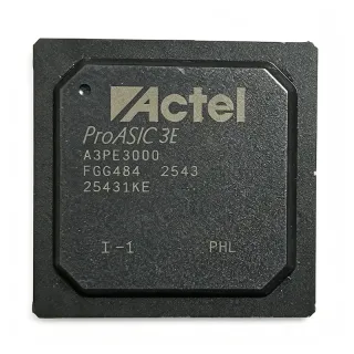
10M16DCF484C8G - MAX 10 FPGA 16K LE 484-BGA | Intel
MPN: 10M16DCF484C8G ✓ Active| Qty | Unit Price | Extended |
|---|---|---|
| 1 | $50.06 | $50.06 |
| 10 | $47.55 | $475.50 |
| 100 | $43.2 | $4,320.00 |
| 500 | $39.5 | $19,750.00 |
| 1,000 | $35.8 | $35,800.00 |
Drop-in alternatives for 10M16DCF484C8G — same package, pin-to-pin compatible. Different-package parts requiring PCB rework are excluded.
Quick Comparison Tool — Select alternative parts for side-by-side comparison:
10M16DCF484C7G
✅ Drop-In✓ In Stock
$31.8 / Unit
View Datasheet →10M16DCF484A7G
✅ Drop-In✓ In Stock
$51 / Unit
View Datasheet →10M16DAF484C7G
✅ Drop-In✓ In Stock
$55.5 / Unit
View Datasheet →10M16DCF484I7G
✅ Drop-In✓ In Stock
$43.95 / Unit
View Datasheet →10M16DAF484I7G
✅ Drop-In✓ In Stock
$60.4 / Unit
View Datasheet →10M16DAF484I7P
✅ Drop-In✓ In Stock
$53.05 / Unit
View Datasheet →10M16DCF484C8G Maximum Ratings & Electrical Characteristics
| Series | MAX 10 |
| Family | MAX 10 |
| Logic Elements | 16000 |
| Embedded Memory (Bits) | 562176 |
| User Flash Memory (Bits) | 516096 |
| Maximum User I/O | 320 |
| DSP Blocks (18x18 Multipliers) | 45 |
| PLLs | 4 |
| Process Technology | 55 nm |
| Supply Voltage (Core) | 1.2 V |
| Package | 484-FBGA |
| Ball Pitch | 1.0 mm |
| Mounting Type | Surface Mount |
| Speed Grade | C8 (commercial, 8 speed grade) |
| Temperature Grade | Commercial (0 C to 85 C) |
| Integrated ADC | Yes, 12-bit SAR |
| Non-volatile Configuration | Yes (dual on-chip flash) |
| RoHS Status | Compliant |
10M16DCF484C8G 484-fbga Pin Configuration Guide
Complete pinout information for 10M16DCF484C8G (484-fbga package). This digital IC includes GPIO, communication interfaces (UART, SPI, I2C), and power pins. Refer to the manufacturer datasheet for alternate pin functions and configuration options. Essential for embedded system design and PCB layout.

No detailed pinout data available for 10M16DCF484C8G.
Refer to the datasheet for full pin configuration.
Safe Operating Area (SOA) & Thermal Characteristics
No official SOA curve available for this digital IC. Always operate within absolute maximum ratings specified in the datasheet. Ensure adequate cooling and derate as needed.
Typical Applications
10M16DCF484C8G is suitable for 6 applications: Industrial Motor Control, Factory Automation I/O Expansion, Video Bridging and Display Controllers, Portable Test and Measurement, Sensor Aggregation Hubs, CPLD Replacement / Glue Logic Aggregation.
Industrial Motor Control
The 10M16DCF484C8G fits industrial motor-control applications because it integrates a 12-bit ADC (for current/voltage sensing), 45 embedded 18x18 multipliers (for Park/Clarke transforms and SVPWM), and 320 user I/O (for multi-axis encoder and resolver feedback). With 16K logic elements it can implement a complete field-oriented control loop for a 3-axis stepper or servo system. Designers typically run the FPGA at 100-150 MHz system clock with a 100 MHz external oscillator; the four on-chip PLLs provide clock-domain flexibility for PWM generation and feedback sampling. The MAX 10 instant-on feature lets the controller begin commutating within milliseconds of power-up, which is critical for safety-rated drives that must reach a safe-torque-off state immediately.
Recommended
Factory Automation I/O Expansion
In factory automation, the 10M16DCF484C8G is used as a programmable I/O concentrator or protocol bridge between field devices (sensors, actuators) and a central PLC. The 320 user I/O can handle dozens of 24 V digital inputs and outputs through external level shifters; the integrated ADC reads analog sensor channels without a dedicated ADC IC. The non-volatile configuration ensures the device boots into the correct personality image immediately, eliminating field-reprogramming concerns after power cycles. Compared with a discrete CPLD design, the FPGA delivers 10-50x more logic capacity at similar cost, while the embedded user flash (516 Kbit) can store calibration data and serial numbers per node. Reference designs from Altera/Intel show typical PROFINET or EtherCAT slave implementations at 50-100 MHz system clock.
Recommended
Video Bridging and Display Controllers
The 10M16DCF484C8G handles video bridging and display-controller tasks by leveraging its LVDS I/O capability (up to 2.5 Gb/s per pair) and sufficient logic to implement timing controllers, color-space converters, and limited scalers. The 484-FBGA package provides enough I/O for parallel RGB, LVDS, or MIPI-DSI interfaces via bridge. Typical use cases include converting DSI to LVDS for industrial displays, generating timing for legacy VGA panels, or fusing multiple camera streams. The 16K logic elements and 45 DSP blocks allow basic chroma resampling and deinterlacing on-the-fly at 1080p60. The four PLLs derive independent pixel clocks from a single reference, simplifying multi-display designs. Power consumption stays below 1.5 W at full throughput thanks to the 55 nm process.
Recommended
Portable Test and Measurement
For portable test-and-measurement instruments such as handheld oscilloscope probes, logic analyzers, or bench multimeters, the 10M16DCF484C8G provides instant-on boot, integrated ADC, and compact BGA packaging in a small footprint. The non-volatile configuration eliminates the boot-PROM cost and PCB area, while the on-chip user flash stores calibration constants and instrument firmware metadata. With 16K LE the FPGA can implement USB protocol, custom trigger logic, and small DSP pre-processing. Typical designs run the FPGA at 50-100 MHz with the on-chip PLL generating multiple clock domains for ADC sampling and USB 2.0 HS. Battery operation is supported through MAX 10's low-power sleep modes, which retain configuration while drawing microamps - ideal for handheld instruments that must wake instantly on button press.
Recommended
Sensor Aggregation Hubs
In IoT edge nodes and sensor aggregation hubs, the 10M16DCF484C8G aggregates data from multiple SPI, I2C, UART, and GPIO-based sensors, performs local preprocessing or filtering, and forwards aggregated data over a high-speed uplink. The 320 user I/O comfortably handle 8-12 SPI slaves or 16+ I2C devices simultaneously; the 45 DSP blocks run basic FIR/IIR filters on accelerometer or microphone streams before forwarding. The embedded ADC samples analog channels (temperature, battery voltage) without a separate IC. The MAX 10 family supports low-power sleep modes that retain state while consuming milliwatts, suitable for battery-powered sensor nodes that wake periodically to transmit.
Recommended
CPLD Replacement / Glue Logic Aggregation
Designers replacing aging CPLD-based glue logic with a more capable FPGA use the 10M16DCF484C8G to consolidate multiple legacy CPLDs into one device. The 16K logic elements absorb wide bus bridges, multi-voltage level shifters, custom reset sequencers, and interrupt controllers that previously required 2-3 separate CPLDs. The integrated ADC adds monitoring of supply rails that CPLDs cannot perform, and the embedded flash stores boot personality for instant-on reset behavior. The 484-BGA package supports the high pin count typical of board-level glue logic (often 100-300 signals). Compared with a multi-CPLD solution, the FPGA reduces PCB area, BOM cost, and power consumption while adding firmware reconfigurability that CPLDs cannot match.
Recommended
Recommended Products Summary
Engineering reference data for 10M16DCF484C8G — comparison, design guidance, and compliance information.
Selection Guide
Comparison with Alternatives
| Parameter | This Product | 10M16DCF484C7G | 10M16DCF484A7G | 10M16DAF484C7G | 10M16DCF484I7G | 10M16DAF484I7G | 10M16DAF484I7P |
|---|---|---|---|---|---|---|---|
| Package | 484-FBGA | 484-FBGA - same | 484-FBGA - same | 484-FBGA - same | 484-FBGA - same | 484-FBGA - same | 484-FBGA - same |
| Brand | Intel | Intel | Intel | Intel | Intel | Intel | Intel |
| Logic Elements | 16000 | 16000 | 16000 | [DATA_NEEDED] | 16000 | [DATA_NEEDED] | [DATA_NEEDED] |
| Speed Grade | C8 | C7 | A7 | C7 | I7 | I7 | I7 |
| Temperature Grade | Commercial (0C to 85C) | Commercial | Commercial | Commercial | Industrial (-40C to 100C) | Industrial | Industrial |
| Embedded Memory (Kbit) | 549 | 549 | 549 | [DATA_NEEDED] | 549 | [DATA_NEEDED] | [DATA_NEEDED] |
| User I/O | 320 | 320 | 320 | 320 | 320 | 320 | 320 |
| Integrated ADC | Yes (12-bit) | Yes (12-bit) | Yes (12-bit) | Yes (12-bit) | Yes (12-bit) | Yes (12-bit) | Yes (12-bit) |
| Non-volatile Configuration | Yes | Yes | Yes | Yes | Yes | Yes | Yes |
Key Differentiators
- Integrated 12-bit ADC not present in Cyclone IV/V E families (vs 10CL025YU256C8G (Cyclone IV E equivalent density))
- Non-volatile instant-on configuration without external boot PROM (vs 10CL025YU256C8G (SRAM-based Cyclone IV E))
- Higher user I/O count in the same package (vs 10M08DCF484C8G (10M08 density, same 484-FBGA))
Design Notes
The 484-FBGA package uses a 1.0 mm ball pitch, which requires PCB fabrication with microvia (laser-drilled) stack-up for fan-out. Use at least a 6-layer PCB with 1 oz copper on outer layers and dedicated inner power/ground planes. Per Intel MAX 10 hardware design guidelines, place 0.1 uF decoupling capacitors on every VCCIO and VCCINT ball pair, with bulk 10-47 uF tantalum or polymer capacitors at each voltage regulator output. Maintain a continuous ground plane under the BGA to provide return-path stitching for high-speed LVDS pairs.
The 484-FBGA package has a theta-JA of approximately 12-15 C/W with the recommended 6-layer PCB layout (estimated: based on typical JEDEC EIA/JESD51 measurement, 484-ball FBGA, 1.0 mm pitch, 6-layer 2s2p board). At maximum toggling activity the FPGA can dissipate 1.5-2.5 W, resulting in a 18-38 C junction temperature rise above ambient. For closed-enclosure industrial designs at 70 C ambient, ensure the FPGA stays below its 85 C commercial junction limit; if not, derate to industrial-grade OPNs such as 10M16DCF484I7G.
Do not confuse the 'DA' feature variant (10M16DAF484) with the 'DC' device (10M16DCF484) - the 'DA' OPNs may have a different mix of logic, memory, and DSP resources, even though they share the same package. Always cross-check the Intel MAX 10 device overview to confirm that the alternative OPN provides the IP blocks and memory depth your design requires. Also note that MAX 10 configuration flash uses dual-image mode by default - if your design relies on fail-safe remote update, configure the image-selection scheme correctly in the Quartus Prime Programming File generator.
Compliance Information
RoHS compliant per Altera/Intel product page (lead-free 'G' suffix in OPN confirms Pb-free ball finish). Not AEC-Q100 qualified; MAX 10 is intended for industrial/commercial use, not automotive. For automotive applications, use a separately-qualified Cyclone IV/V automotive-grade part.