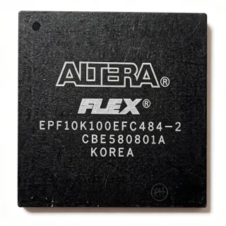
EP2S15F484I4N - 15K Logic FPGA, 484-BGA | Intel
MPN: EP2S15F484I4N ✗ End of Life| Qty | Unit Price | Extended |
|---|---|---|
| 1 | $224.6325 | $224.63 |
| 10 | $0 | $0.00 |
| 100 | $0 | $0.00 |
| 500 | $0 | $0.00 |
| 1,000 | $0 | $0.00 |
EP2S15F484I4N Overview
A field-programmable gate array is a programmable semiconductor device built from configurable logic blocks, routing resources, input/output elements, and often embedded memory and DSP-oriented blocks. FPGA devices sit within the broader hierarchy of programmable logic devices, digital integrated circuits, and semiconductors. Engineers configure the logic and interconnect to implement control, communications, interface, and signal-processing functions after fabrication, enabling design changes without a new silicon mask set.
The key electrical and physical characteristics include 15,600 logic elements, 419,328 memory bits, 342 I/O pins, 484 BGA balls, and a 1.2 V operating voltage. The large logic capacity and embedded memory allow parallel digital functions and data buffering within one package. The 342 I/O pins provide broad connectivity for external buses, control signals, and high-speed interfaces. The fine-pitch BGA format supports dense board routing but requires controlled assembly and reliable thermal design.
The device belongs to the Stratix II FPGA family and is associated with 780 configurable logic blocks in the supplied distributor and comparison data. Its architecture is intended for configurable digital implementation rather than fixed application-specific processing. The combination of logic resources and embedded memory can be used for register-intensive designs, protocol handling, state machines, and interface bridging. Exact performance values such as maximum clock frequency, transceiver count, operating temperature limits, package dimensions, and supported I/O standards are not present in the supplied verified text and therefore require datasheet verification.
Typical applications include industrial control, communications equipment, test and measurement, data acquisition, digital signal processing, and embedded systems. The 15,600 logic elements and 419,328 memory bits suit designs requiring substantial programmable logic and local storage, while 342 I/O pins support external memory, converters, processors, and peripheral interfaces. The 484-BBGA package is appropriate for space-constrained systems that need high connection density.
A primary design consideration is that BGA assembly requires precise land-pattern implementation, via-in-pad or escape routing planning, controlled impedance where applicable, and thermal analysis. Before production, confirm pin assignments, voltage tolerances, configuration requirements, clock limits, and industrial temperature limits from the manufacturer datasheet. This page combines verified distributor specifications, compatible-device guidance, comparison parameters, and engineering design considerations to support part selection and BOM review.
Drop-in alternatives for EP2S15F484I4N — same package, pin-to-pin compatible. Different-package parts requiring PCB rework are excluded.
Variants in this series
Same-series models that are drop-in compatible with EP2S15F484I4N (same form factor and footprint) — differing in Speed Grade, Package, Family, Operating Temperature, Adaptive Logic Modules (ALMs).
Quick Comparison Tool — Select alternative parts for side-by-side comparison:
EP2S15F484I4
✅ Drop-In✓ In Stock
$253.03 / Unit
View Datasheet →EP2S15F484C4N
✅ Drop-In✓ In Stock
$185 / Unit
View Datasheet →EP2S15F484C4
✅ Drop-In✓ In Stock
$205 / Unit
View Datasheet →EP2S15F484C3N
✅ Drop-In✓ In Stock
$155 / Unit
View Datasheet →EP2S15F484C3
✅ Drop-In✓ In Stock
$118 / Unit
View Datasheet →EP2S15F484I4N Maximum Ratings & Electrical Characteristics
| Device Type | Field Programmable Gate Array (FPGA) |
| Family | Stratix II |
| Logic Elements | 15,600 |
| Embedded Memory | 419,328 bits |
| User I/O Pins | 342 |
| Configurable Logic Blocks | 780 |
| Operating Voltage | 1.2 V |
| Package | 484-BBGA |
| Terminal Count | 484 |
| Terminal Form | Ball |
| Package Shape | Square |
| Temperature Grade | Industrial |
| Mounting Type | Surface Mount |
EP2S15F484I4N square Pin Configuration Guide
Pin configuration for EP2S15F484I4N (square package). This digital IC includes GPIO, communication interfaces (UART, SPI, I2C), and power pins. Refer to the manufacturer datasheet for alternate pin functions and configuration options. Essential for embedded system design and PCB layout.

No detailed pinout data available for EP2S15F484I4N.
Refer to the datasheet for full pin configuration.
Typical Applications
EP2S15F484I4N is suitable for 6 applications: Industrial Control Systems, Communications Equipment, Test and Measurement, Data Acquisition and Processing, Digital Signal Processing, Legacy Embedded Computing.
Industrial Control Systems
EP2S15F484I4N fits industrial control systems that require substantial programmable logic and a high-density interconnect package. The verified 15,600 logic elements, 780 configurable logic blocks, and 342 I/O pins support motor-control sequencing, sensor aggregation, safety-state logic, and communication between controllers and actuators. Its industrial temperature grading makes it a relevant candidate for equipment exposed to demanding operating conditions, although the exact temperature limits must be confirmed. The 484-BBGA package provides 484 terminals for power, clocks, configuration, and I/O, but it requires a carefully designed escape-routing strategy. Use the FPGA for deterministic parallel processing, protocol conversion, and hardware control functions while preserving firmware flexibility. The 1.2 V supply requirement should be implemented with a low-noise power tree and verified sequencing.
Recommended
Communications Equipment
EP2S15F484I4N is suitable for communications equipment requiring programmable packet processing, interface adaptation, and parallel digital logic. The 15,600 logic elements and 419,328 embedded memory bits can support protocol state machines, framing, buffering, lookup operations, and traffic-management functions. Its 342 user I/O pins allow connections to line-interface devices, network processors, converters, and external memory. Because the supplied data does not state a verified maximum clock frequency or transceiver specification, the device should be selected only after timing analysis and interface validation. The 484-BBGA package supports high pin density but demands controlled impedance, continuous reference-plane design, and reliable power delivery. A 1.2 V core rail should be generated with suitable decoupling and monitored for startup sequencing.
Recommended
Test and Measurement
EP2S15F484I4N can support test and measurement platforms that need deterministic acquisition, triggering, sequencing, and data formatting. The verified 15,600 logic elements and 419,328 embedded memory bits provide resources for parallel channel processing, counters, capture buffers, and instrument-control state machines. The 342 I/O pins enable connection to analog-to-digital converters, digital-to-analog converters, sensors, and host processors. In this application, the FPGA can reduce host-processor workload by performing time-critical operations in hardware. The 1.2 V supply and 484-BBGA package require careful low-noise power and PCB layout. The supplied data does not specify I/O standards, signal-integrity limits, or timing performance, so those values must be obtained from the manufacturer datasheet before schematic and layout sign-off.
Recommended
Data Acquisition and Processing
EP2S15F484I4N fits data-acquisition systems where multiple digital channels must be captured, buffered, filtered, formatted, and transferred to a host. The 15,600 logic elements support parallel datapaths and control logic, while the verified 419,328 memory bits provide embedded storage for intermediate samples and protocol data. The 342 user I/O pins are useful for connecting converters, clock sources, memory devices, and high-speed host interfaces. The industrial temperature grading is relevant for measurement equipment deployed in controlled or harsh industrial environments. Because the verified data does not specify maximum clock frequency, supported I/O standards, or power consumption, the FPGA design must be validated against the selected converter timing and signal-integrity requirements. The 484-BBGA package requires controlled assembly and thorough thermal analysis.
Recommended
Digital Signal Processing
EP2S15F484I4N can implement configurable digital signal-processing functions in embedded and industrial systems. Its 15,600 logic elements and 419,328 embedded memory bits are appropriate for parallel filtering, data formatting, control loops, and buffering, while 342 I/O pins support external converters and memory. The FPGA is useful when processing must be deterministic and hardware-parallel rather than dependent on a general-purpose processor. Exact DSP block count, multiplier performance, maximum clock rate, and supported arithmetic throughput are not provided in the verified data, so performance claims must not be inferred. Validate the design using the manufacturer timing documentation and application-specific simulations. The 1.2 V rail should have low-noise decoupling, and the 484-BBGA layout should provide short power paths, continuous references, and adequate thermal spreading.
Recommended
Legacy Embedded Computing
EP2S15F484I4N is relevant for maintaining and extending legacy embedded computing systems built around the Intel Stratix II family. The device provides 15,600 logic elements, 780 configurable logic blocks, 419,328 embedded memory bits, and 342 user I/O pins in a 484-BBGA package. These resources can support board-level control, bus interfaces, protocol handling, and replacement of obsolete fixed-function logic. The part is an obsolete or legacy family member according to the supplied search context, so long-term availability, counterfeit risk, and lifecycle planning require procurement review. The 1.2 V supply and BGA assembly requirements make redesign difficult, and replacement must be validated at the pin, timing, configuration, and software-tool levels. Use EP2S15F484I4 as the primary equivalent candidate, subject to exact manufacturer ordering-code verification.
Recommended
Recommended Products Summary
Engineering reference data for EP2S15F484I4N — comparison, design guidance, and compliance information.
Selection Guide
Comparison with Alternatives
| Parameter | This Product | EP2S15F484I4 | EP2S15F484C4N | EP2S15F484C4 | EP2S15F484C3N | EP2S15F484C3 |
|---|---|---|---|---|---|---|
| Brand | Intel | Intel | Intel | Intel | Intel | Intel |
| Package | 484-BBGA | 484-BBGA | 484-BBGA | 484-BBGA | 484-BBGA | 484-BBGA |
| Package Pin Count | 484 | 484 | 484 | 484 | 484 | 484 |
| Lifecycle Status | Obsolete or legacy family member | Likely same legacy family; exact status not supplied | Likely same legacy family; exact status not supplied | Likely same legacy family; exact status not supplied | Likely same legacy family; exact status not supplied | Likely same legacy family; exact status not supplied |
Key Differentiators
- Verified direct equivalent candidate (vs EP2S15F484I4)
- Same-package alternative for evaluation (vs EP2S15F484C4N)
- High verified I/O and logic capacity (vs EP2S15F484C3N)
Design Notes
EP2S15F484I4N is specified at 1.2 V, so the regulator must provide a stable core rail with appropriate transient response and decoupling. Place the bulk and local ceramic capacitors close to the relevant power and ground balls using the manufacturer reference design. Confirm the allowed supply tolerance, current demand, ramp rate, and power-up sequence from the datasheet; these values are not present in the supplied verified data. Do not release the board until the regulator tolerance and FPGA limits are compared under worst-case load and temperature.
The 484-BBGA package has high connection density and requires thermal planning even when the available data does not state power consumption or thermal resistance. Estimate board-level power from the actual configuration and toggle rate after the design is available, then confirm junction temperature using the package thermal model. Use a continuous ground or power-reference plane, thermal vias where appropriate, and sufficient copper spreading around the BGA. Exact junction-to-ambient resistance, maximum junction temperature, and thermal derating are not supplied and must be obtained from the manufacturer documentation.
Before routing EP2S15F484I4N, obtain the official 484-ball pin assignment and package land pattern. The 342 user I/O pins do not map one-to-one to all 484 balls because power, clock, configuration, ground, and reserved functions also use package terminals. Verify escape routing, via construction, BGA pad geometry, solder-mask rules, and assembly capability with the PCB fabricator. Keep high-speed traces over a continuous reference plane and calculate the required layer count from the complete ball map rather than from the user-I/O count alone.
Do not treat an ordering-code similarity as proof of drop-in equivalence. EP2S15F484I4, EP2S15F484C4N, and related candidates are listed with the same 484-BBGA family context, but the supplied data does not confirm every timing, electrical, temperature, configuration, or software-tool characteristic. Compare official ordering tables, pinouts, timing models, voltage limits, and lifecycle documents. For legacy production, retain the existing configuration bitstream, tool versions, and board-level test fixtures until equivalence is demonstrated on hardware.
Compliance Information
Compliance information is not included in the supplied verified web data. AEC-Q100 status is not stated; do not infer automotive qualification from industrial temperature grading.