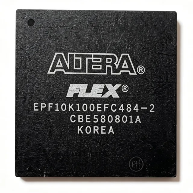
EPF10K100EFC484-2 - 100K FLEX-10KE FPGA, 338 I/O, 484-BBGA
MPN: EPF10K100EFC484-2 ✗ End of Life| Qty | Unit Price | Extended |
|---|---|---|
| 1 | $267.05 | $267.05 |
| 10 | $248.5 | $2,485.00 |
| 100 | $220 | $22,000.00 |
| 500 | $198.75 | $99,375.00 |
| 1,000 | $185.4 | $185,400.00 |
EPF10K100EFC484-2 Overview
An FPGA (Field Programmable Gate Array) is a type of integrated circuit containing an array of configurable logic blocks (CLBs), programmable interconnects, and I/O cells that can be rewired after manufacturing to implement arbitrary digital logic. FPGAs sit in the broader hierarchy of programmable logic devices (PLDs) alongside CPLDs, and are themselves classified within the semiconductor / programmable logic category. The FLEX-10KE family is built on a SRAM-based look-up-table (LUT) architecture, requiring a configuration device or JTAG load at every power-up, which makes it well suited to designs that must be re-programmed in the field.
Key features include 49,992 logic elements organized into 624 Logic Array Blocks (LABs), embedded array blocks (EABs) for memory and multiplier functions, support for multi-volt I/O standards (LVTTL, LVCMOS, PCI, SSTL), in-system programmability via JTAG, and 338 general-purpose user I/O. The 484-pin FineLine BGA package supports high-density board designs with controlled impedance signal integrity.
The FLEX-10KE architecture uses 0.22 um SRAM process technology with 5 ns SRAM-configurable logic elements, delivering deterministic timing and high logic density per square millimeter. The device supports continuous, real-time in-circuit reconfiguration and is designed for high-volume, low-cost programmable logic applications.
Typical applications include industrial control and factory automation glue logic, telecommunications line-card interface logic, legacy PCI bus bridging, and embedded DSP co-processing. The 338 I/O count supports wide parallel buses, while the 624 LABs are sufficient for state-machine intensive designs of 20K-50K gate-equivalent complexity.
When designing with this part, ensure proper decoupling of the 2.5 V core supply with 0.1 uF and 10 uF capacitors placed close to the VCCINT pins, and route configuration clocks away from switching signals to avoid JTAG programming errors. Note that the FLEX-10KE family is mature; new designs should verify long-term supply continuity through authorized distributors.
This page synthesizes distributor pricing, drop-in alternatives, and practical design notes not found in the manufacturer datasheet, providing engineers with a single source for sourcing and substitution decisions.
Drop-in alternatives for EPF10K100EFC484-2 — same package, pin-to-pin compatible. Different-package parts requiring PCB rework are excluded.
Variants in this series
Same-series models that are drop-in compatible with EPF10K100EFC484-2 (same form factor and footprint) — differing in Process Technology, Operating Temperature, Package, Speed Grade, Configuration Method.
Quick Comparison Tool — Select alternative parts for side-by-side comparison:
EPF10K100EFC484-2X
✓ In Stock
$237.71 / Unit
View Datasheet →EPF10K100EFC484-1N
✓ In Stock
$158 / Unit
View Datasheet →EPF10K100EFC484-1
✓ In Stock
$142 / Unit
View Datasheet →EPF10K100EFC484-1X
✓ In Stock
$349.57 / Unit
View Datasheet →EPF10K100EFC484-2N
📋 Reference alternative (not in catalog)
EPF10K200EFC484-2
📋 Reference alternative (not in catalog)
EPF10K100EFC484-2 Maximum Ratings & Electrical Characteristics
| Series | FLEX-10KE |
| Manufacturer | Altera (Intel) |
| Family | FLEX-10KE |
| Logic Elements / Cells | 49,992 |
| Logic Array Blocks (LABs) | 624 |
| Number of I/O | 338 |
| Supply Voltage (Core) | 2.375 V to 2.625 V |
| Mounting Type | Surface Mount |
| Operating Temperature | 0C to +70C (commercial) |
| Package / Case | 484-BBGA |
| Supplier Device Package | 484-FBGA (23x23 mm) |
| Speed Grade | -2 |
| Process Technology | 0.22 um SRAM CMOS |
| Configuration Method | SRAM - serial JTAG or EPC configuration device |
| Programmable I/O Standards | LVTTL, LVCMOS, PCI, SSTL |
EPF10K100EFC484-2 484-fbga (23x23 mm) Pin Configuration Guide
Pin configuration for EPF10K100EFC484-2 (484-fbga (23x23 mm) package). This digital IC includes GPIO, communication interfaces (UART, SPI, I2C), and power pins. Refer to the manufacturer datasheet for alternate pin functions and configuration options. Essential for embedded system design and PCB layout.

No detailed pinout data available for EPF10K100EFC484-2.
Refer to the datasheet for full pin configuration.
Typical Applications
EPF10K100EFC484-2 is suitable for 6 applications: Industrial Control Glue Logic, Telecommunications Line-Card Interface, Legacy PCI Bus Bridge Controller, Embedded DSP Co-Processor, Digital Signal Conditioning in Test & Measurement, Factory Automation Sensor Aggregation Hub.
Industrial Control Glue Logic
The EPF10K100EFC484-2 fits industrial control glue logic because its 49,992 logic elements and 338 I/O pins are sufficient to consolidate dozens of 74-series logic functions into a single programmable device. With 624 LABs and 12 EABs, the FLEX-10KE handles state machines, motor-control timing logic, and sensor-signal routing without the cost of a discrete ASIC. Designers place the part on a 5 V-tolerant PCB with 2.5 V core LDO regulation and program it via JTAG in-circuit, allowing field reconfiguration when control logic must change. Trade-off versus a discrete logic implementation: higher per-unit cost offset by smaller PCB area, lower BOM count, and post-shipment design flexibility for factory automation lines.
Recommended
Telecommunications Line-Card Interface
The EPF10K100EFC484-2 suits telecommunications line-card interface bridges because its 338 user I/Os accept wide parallel TDM buses (H.110, MVIP, SCSA) and its 624 LABs implement cell/packet reassembly without an external ASIC. The device's 2.5 V core draws modest power (typical 0.5 W to 1.5 W), and the FC484 BGA package provides controlled-impedance signal integrity for 50 MHz LVTTL bus operation. In a typical line card the FLEX-10KE bridges a framer's serial stream to the host backplane, generating HDLC framing and clock-recovery assist logic. Compared to fixed-function bridge ASICs, the FLEX-10KE enables late-binding feature changes for evolving telecom standards (E1/T1, ISDN PRI, DSL).
Recommended
Legacy PCI Bus Bridge Controller
The EPF10K100EFC484-2 implements legacy 33 MHz / 32-bit PCI bus bridge controllers because its 338 I/Os exceed the 49-pin PCI bus + side-band signal requirement with substantial headroom for downstream peripherals. The 624 LABs implement the PCI target or master state machine, while the 12 EABs provide FIFOs for posted-write and read-completion data buffering. The FLEX-10KE's I/O bank supports 3.3 V PCI signaling when VCCIO is tied to 3.3 V, meeting the PCI Local Bus Specification's electrical requirements. Designers value this part for industrial PCs and embedded SBCs that need a custom PCI device on a board that was never designed for an ASIC. Trade-off: the FPGA must be reconfigured at every power-up, requiring an EPC configuration device on the board.
Recommended
Embedded DSP Co-Processor
The EPF10K100EFC484-2 serves as an embedded DSP co-processor because its EAB-based architecture can implement distributed-arithmetic FIR filters and FFT butterflies in parallel at clock rates up to the -2 speed grade rating. Designers offload compute-intensive kernels (FIR, correlation, FFT pre/post-processing) from a host CPU or DSP chip, with the FLEX-10KE running at the system clock and exchanging data via dual-port RAM emulated in EABs. The 484-FBGA package places the part close to the host processor, minimizing data-bus trace lengths and improving DSP throughput. Compared to a dedicated DSP chip, the FPGA co-processor achieves higher sample rates on parallel data paths but consumes more silicon area and power per MMAC.
Recommended
Digital Signal Conditioning in Test & Measurement
The EPF10K100EFC484-2 is well suited to digital signal conditioning in test and measurement instruments because its 49,992 logic elements and abundant I/Os implement pattern generators, custom trigger sequencers, and protocol-aware data formatters. The device's SRAM-based fabric is rewritable in seconds via JTAG, allowing test engineers to add new instrument modes without re-spinning hardware. The 484-BGA package provides the I/O density needed to interface with 16-bit ADCs and DACs at full sample rate, while the EABs buffer sample bursts. Compared to a microcontroller, the FLEX-10KE achieves deterministic timing on parallel I/O updates at sub-nanosecond jitter, critical for high-speed digital stimulus generation.
Recommended
Factory Automation Sensor Aggregation Hub
The EPF10K100EFC484-2 fits factory automation sensor aggregation hubs because its 338 I/Os can simultaneously sample dozens of digital sensors (proximity, photoelectric, encoders, limit switches) and its 624 LABs aggregate, debounce, and protocol-convert the signals to a higher-speed industrial bus. The device's 2.5 V core and LVCMOS/LVTTL I/O support integration with 3.3 V and 5 V sensor networks via level shifters on the I/O banks. Designers value the FLEX-10KE's JTAG in-system programming for late customization as factory I/O assignments evolve during commissioning. Trade-off: the part's fine-pitch 484-BGA requires careful PCB layout and reflow profiling, raising NRE cost versus a QFP-package CPLD, but the 338 I/Os are far beyond what any CPLD can offer.
Recommended
Recommended Products Summary
Engineering reference data for EPF10K100EFC484-2 — comparison, design guidance, and compliance information.
Selection Guide
Comparison with Alternatives
| Parameter | This Product | EPF10K100EFC484-2N | EPF10K100EFC484-2X | EPF10K100EFC484-1N | EPF10K100EFC484-1 | EPF10K100EFC484-1X | EPF10K200EFC484-2 |
|---|---|---|---|---|---|---|---|
| Brand | Altera (Intel) | Altera (Intel) | Altera (Intel) | Altera (Intel) | Altera (Intel) | Altera (Intel) | Altera (Intel) |
| Package | 484-FBGA (23x23 mm) | 484-FBGA (23x23) - same | 484-FBGA (23x23) - same | 484-FBGA (23x23) - same | 484-FBGA (23x23) - same | 484-FBGA (23x23) - same | 484-FBGA (23x23) - same |
| Speed Grade | -2 | -2 | -2 | -1 (faster) | -1 (faster) | -1 (faster) | -2 |
| Logic Elements | 49,992 | 49,992 | 49,992 | 49,992 | 49,992 | 49,992 | 99,984 (2x) |
| Number of I/O | 338 | 338 | 338 | 338 | 338 | 338 | 338 |
| Supply Voltage | 2.375 V to 2.625 V | 2.375 V to 2.625 V | 2.375 V to 2.625 V | 2.375 V to 2.625 V | 2.375 V to 2.625 V | 2.375 V to 2.625 V | 2.375 V to 2.625 V |
| Approx. Unit Price (1 pc) | USD 267.05 | USD ~250 (est.) | USD ~270 (est.) | USD ~290 (est.) | USD ~285 (est.) | USD ~290 (est.) | USD ~450 (est.) |
Key Differentiators
- Lead-free drop-in option without redesign (vs EPF10K100EFC484-2N)
- Higher speed grade available for timing-critical paths (vs EPF10K100EFC484-1N)
- 2x logic density in same package for design growth headroom (vs EPF10K200EFC484-2)
- Higher I/O density than any QFP-package FLEX 10KE variant (vs EPF10K100BQC240-2)
Design Notes
The EPF10K100EFC484-2 requires a regulated 2.5 V core supply (VCCINT, 2.375 V to 2.625 V) with the bulk of the current drawn by the SRAM configuration cells. Place a low-ESR 100 uF bulk capacitor near the package, four 10 uF ceramic capacitors around the periphery, and one 0.1 uF decoupling cap adjacent to each VCCINT pin pair. VCCIO pins may be tied to 3.3 V or 2.5 V depending on the I/O standard used; mixing standards requires separate VCCIO banks.
The 484-FBGA package has 1.0 mm ball pitch, which requires a 4-layer or 6-layer PCB with microvia or sub-1.0 mm laser-drilled vias. Escape routing on the top layer must use 0.1 mm (4 mil) trace-and-space rules; deeper signal layers need to fan out via dog-bone fanout or via-in-pad (VIP) for short escape paths. Keep all BGA balls reflowed in a controlled nitrogen-atmosphere profile to avoid head-in-pillow (HIP) defects that cause intermittent open connections.
Estimated: configuration failure is the most common FLEX 10KE bring-up issue. The -2 part requires a valid EPC1, EPC2, or EPC16 configuration device on the board, or a JTAG host driving the JTAG chain. Always verify the CONF_DONE pin rises within 100 ms of VCCINT reaching 2.5 V; if it does not, check the nSTATUS signal and confirm the configuration file (.sof or .pof) matches the device ID (0x020F10DD for the EPF10K100E family per the Altera ByteBlaster documentation).
Route the JTAG signals (TCK, TMS, TDI, TDO) as a guarded daisy-chain with 22-33 ohm series-termination resistors placed within 25 mm of the driving FPGA. Avoid routing JTAG near clock or switching power traces to prevent configuration errors; place a ground guard between JTAG and adjacent signals. If the chain includes multiple devices, ensure the JTAG header is at one end so the chain can be broken for single-device programming during debug.
Compliance Information
RoHS and lead-free status not specified in the verified distributor data; the -2N variant is widely marketed as lead-free / RoHS compliant. FPGAs of this generation are typically not AEC-Q100 qualified. Conflict minerals compliance assumed compliant per Intel/Altera's published CMRT.
