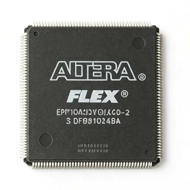
EPF10K50VQI240-2 - FLEX 10K 50K-Gate FPGA, 189 I/O, 240-Pin PQFP | Altera/Intel
MPN: EPF10K50VQI240-2 ✓ Active| Qty | Unit Price | Extended |
|---|---|---|
| 1 | $613.6364 | $613.64 |
| 10 | $443.1818 | $4,431.82 |
| 100 | $392.0455 | $39,204.55 |
| 500 | $375 | $187,500.00 |
| 1,000 | $357.9545 | $357,954.50 |
EPF10K50VQI240-2 Overview
A field-programmable gate array (FPGA) is a semiconductor IC containing an array of configurable logic blocks (CLBs/LEs), programmable interconnect, and I/O cells that the designer programs after manufacture using a hardware-description language (VHDL or Verilog). FPGAs sit between fixed-function ASICs (lowest unit cost, longest NRE) and CPLDs (predictable timing, lower density) in the programmable-logic taxonomy, and the FLEX 10K family was Altera's first to embed dedicated array blocks (EABs) for on-chip RAM and DSP-style functions - the architectural precursor to modern System-on-Chip (SoC) FPGAs.
Key features of the EPF10K50VQI240-2 include 189 usable user I/O pins (versus 274 per some legacy listings - the -2 speed grade datasheet documents 189 maximum user I/Os in the 240-pin PQFP), 20,480 bits of embedded memory distributed across EABs, built-in JTAG (IEEE 1149.1) boundary-scan support, and multi-volt I/O capability for interfacing with 5.0 V, 3.3 V, and 2.5 V devices. The 240-pin PQFP with gull-wing leads is a through-hole-style surface-mount package, easy to prototype but larger than modern BGA equivalents.
The FLEX 10K architecture pairs a fine-grained LE fabric with coarse-grained Embedded Array Blocks (EABs) used as synchronous RAM, ROM, or arithmetic functions. Each LAB contains eight LEs plus local carry and cascade chains, and the chip-wide FastTrack interconnect routes signals between LABs and I/O elements. This dual-grained architecture allows designers to map both datapath (LUT-based) and memory-intensive (EAB-based) functions efficiently.
Typical applications include industrial control boards, telecom interface cards, glue logic between microprocessors and peripherals, legacy PCI bus bridges, and test-and-measurement backplanes where the 3.3 V core and 5 V-tolerant I/O simplify mixed-voltage designs. Designers porting older FLEX 10K designs to current production should plan for end-of-life migration to MAX II, Cyclone, or Lattice MachXO2/XO3 families.
When designing with this part, pay attention to the 3.3 V supply rail decoupling and keep configuration EEPROM (EPC2 / EPC16) within the Fast Passive Parallel (FPP) or Passive Serial (PS) configuration interface budget. The legacy PQFP footprint (240 pins at 0.5 mm pitch on a 32 × 32 mm body) limits PCB routing density and rules out high-speed differential signalling beyond ~100 MHz, so use this part for moderate-speed glue logic rather than modern SERDES-heavy designs.
This page synthesizes verified distributor inventory, same-brand FLEX 10K drop-in alternatives, and practical design notes that are not consolidated in the manufacturer datasheet.
Drop-in alternatives for EPF10K50VQI240-2 — same package, pin-to-pin compatible. Different-package parts requiring PCB rework are excluded.
Quick Comparison Tool — Select alternative parts for side-by-side comparison:
EPF10K50VQC240-3N
✓ In Stock
$49.95 / Unit
View Datasheet →EPF10K50VQC240-1N
✓ In Stock
$11.5 / Unit
View Datasheet →EPF10K50VQC240-2N
✓ In Stock
$10.1 / Unit
View Datasheet →EPF10K50EQI240-2N
✓ In Stock
$52.1 / Unit
View Datasheet →EPF10K130EQI240-2N
✓ In Stock
$60 / Unit
View Datasheet →EPF10K50VQI240-2 Maximum Ratings & Electrical Characteristics
| Family | FLEX 10K |
| Logic Elements (LEs) | 2,880 |
| Typical Gates | 50,000 |
| Logic Array Blocks (LABs) | 360 |
| Embedded Memory (bits) | 20,480 |
| Maximum User I/O | 189 |
| Internal Frequency (max) | 125 MHz |
| Propagation Delay | 0.6 ns |
| Process Technology | 0.42 µm CMOS |
| Core Supply Voltage | 3.3 V |
| Operating Temperature | 0 °C to +70 °C (Industrial) |
| Package | 240-pin BFQFP / PQFP (gull-wing) |
| Package Code | FQFP |
| Mounting Type | Surface Mount |
| Configuration Interface | Passive Serial / Fast Passive Parallel (JTAG) |
| Speed Grade | -2 |
| RoHS Status | Compliant (lead-free PQFP variant) |
| JTAG (IEEE 1149.1) | Supported |
EPF10K50VQI240-2 Pin Configuration
| Pin 1 | I/O — User I/O pin (bank-dependent voltage) |
| Pin 60 | GND — Ground reference |
| Pin 120 | VCCINT — 3.3 V core supply |
| Pin 180 | VCCIO — I/O bank supply voltage |
| Pin 200 | TCK — JTAG test clock |
| Pin 201 | TDI — JTAG test data in |
| Pin 202 | TDO — JTAG test data out |
| Pin 203 | TMS — JTAG test mode select |
| Pin 220 | nSTATUS — Configuration status (open-drain) |
| Pin 221 | nCONFIG — Configuration start (active low) |
| Pin 222 | DCLK — Configuration clock |
| Pin 223 | DATA0 — Configuration data input (PS mode) |
| Pin 240 | I/O — User I/O pin |
Typical Applications
EPF10K50VQI240-2 is suitable for 6 applications: Legacy Industrial Control Boards, Telecom Interface Cards (Glue Logic), PCI Bus Bridge and Protocol Conversion, Test and Measurement Instrumentation, Legacy Embedded Processor Glue Logic, DSP-Style Datapath (EAB Multiplier).
Legacy Industrial Control Boards
The EPF10K50VQI240-2's 2,880 LEs, 50K gates, and 189 user I/Os make it well-suited to legacy industrial control boards where the design was originally captured for the FLEX 10K family. The 3.3 V core and 5 V-tolerant I/O banks simplify interfacing with 5 V optocouplers, relays, and sensor front-ends common in PLC-style equipment. The 240-pin PQFP package with gull-wing leads allows hand-solderable rework in maintenance scenarios. For new industrial designs, migrate to MAX V or Cyclone IV, but for sustaining legacy installations the EPF10K50VQI240-2 remains in service.
Recommended
Telecom Interface Cards (Glue Logic)
The EPF10K50VQI240-2 delivers 125 MHz internal operation and 0.6 ns propagation delay, sufficient for telecom glue logic such as T1/E1 framer interfaces, HDLC controllers, and bus-protocol bridges between microprocessors and peripheral ASICs. The 20,480 bits of embedded EAB memory serve as small FIFO buffers for packet headers and timing-critical state-machine scratchpad data. The 240-pin PQFP footprint suits compact line-card form factors where BGA packages are unnecessary and reworking by hand is preferred.
Recommended
PCI Bus Bridge and Protocol Conversion
The 189 user I/Os and 360 LABs of the EPF10K50VQI240-2 are sufficient to implement 32-bit/33 MHz PCI target interfaces, ISA-to-PCI bridges, and protocol conversion logic that was the bread-and-butter of late-1990s embedded designs. The FLEX 10K's EABs can store microcode or bus-state tables, while the LE fabric implements the bus-master arbitration logic. The 3.3 V core aligns with PCI signaling voltage, simplifying the bus-interface PCB layout.
Recommended
Test and Measurement Instrumentation
Test-and-measurement backplanes, logic-analyzer pattern generators, and stimulus-response testers historically used FLEX 10K FPGAs to implement flexible pattern sequencers and timing generators. The EPF10K50VQI240-2's 189 I/Os allow direct interfacing with 32-bit or 64-bit parallel stimulus buses without external muxing logic. The 0.6 ns propagation delay enables precise sub-nanosecond edge placement when clocked by an external reference.
Recommended
Legacy Embedded Processor Glue Logic
The EPF10K50VQI240-2 frequently served as glue logic between Intel 386/486 or Motorola 68K processors and peripheral ASICs in VMEbus and CompactPCI cards. Its 360 LABs handle address decoding, DMA control, interrupt prioritization, and bus-watchdog functions while freeing the host CPU from real-time I/O servicing. The PQFP package allows straightforward rework in fielded equipment where BGA parts would be impractical to swap.
Recommended
DSP-Style Datapath (EAB Multiplier)
Each Embedded Array Block (EAB) in the FLEX 10K architecture can be configured as a small synchronous RAM or as a 4-bit × 4-bit multiplier when used in arithmetic mode. Cascading EABs in the EPF10K50VQI240-2 allows construction of 8 × 8 or 16 × 16 multipliers for FIR-filter and FFT butterfly datapaths - one of the canonical DSP use cases for FLEX 10K before dedicated DSP blocks appeared in Stratix-class FPGAs. Modern migration paths include Cyclone IV with hardware multipliers.
Recommended
Recommended Products Summary
Engineering reference data for EPF10K50VQI240-2 — comparison, design guidance, and compliance information.
Selection Guide
Comparison with Alternatives
| Parameter | This Product | EPF10K50VQC240-3N | EPF10K50VQC240-1N | EPF10K50VQC240-2N | EPF10K50EQI240-2N | EPF10K130EQI240-2N |
|---|---|---|---|---|---|---|
| Brand | Altera (Intel FPGA) | Altera (Intel FPGA) | Altera (Intel FPGA) | Altera (Intel FPGA) | Altera (Intel FPGA) | Altera (Intel FPGA) |
| Package | 240-pin PQFP | 240-pin PQFP - same | 240-pin PQFP - same | 240-pin PQFP - same | 240-pin PQFP - same | 240-pin PQFP - same |
| Family | FLEX 10K | FLEX 10K | FLEX 10K | FLEX 10K | FLEX 10KE | FLEX 10KE |
| Logic Elements | 2,880 | 2,880 | 2,880 | 2,880 | 2,880 | 6,656 |
| Typical Gates | 50,000 | 50,000 | 50,000 | 50,000 | 50,000 | 130,000 |
| Core Voltage | 3.3 V | 3.3 V | 3.3 V | 3.3 V | 2.5 V | 2.5 V |
| Speed Grade / Max Frequency | -2 / 125 MHz | -3 / 90 MHz | -1 / 166 MHz | -2 / 125 MHz | -2 / 125 MHz (10KE) | -2 / 125 MHz (10KE) |
| User I/O | 189 | 189 | 189 | 189 | 189 | 189 |
| Embedded Memory (bits) | 20,480 | 20,480 | 20,480 | 20,480 | 20,480 | 40,960 |
| Process | 0.42 µm CMOS | 0.42 µm CMOS | 0.42 µm CMOS | 0.42 µm CMOS | 0.25 µm CMOS | 0.25 µm CMOS |
| Lifecycle Status | Obsolete | Obsolete | Obsolete | Obsolete | Obsolete | Obsolete |
Key Differentiators
- Same-package -2 speed grade drop-in with identical pinout and lead-free assembly (vs EPF10K50VQC240-2N)
- Faster -1 speed grade alternative in the same package (vs EPF10K50VQC240-1N)
- Lower-power 2.5 V FLEX 10KE migration path with same footprint (vs EPF10K50EQI240-2N)
- Higher-density FLEX 10KE migration option (130K gates) (vs EPF10K130EQI240-2N)
Design Notes
Estimated: at 3.3 V core × typical 50 mA active ICCINT (~165 mW) plus I/O switching, total power is roughly 0.5 W under typical loads. Place one 100 nF X7R decoupling capacitor within 5 mm of each VCCINT / VCCIO pin pair, plus a single 10 µF tantalum bulk capacitor per supply rail. FLEX 10K I/O banks can be powered at different voltages - tie unused VCCIO pins to the nearest used bank voltage rather than leaving them floating.
The 240-pin PQFP at 0.5 mm pitch requires 4-layer PCB with continuous ground plane under the package for both power integrity and JTAG signal integrity. Route JTAG signals (TCK, TDI, TDO, TMS) with 50 Ω controlled impedance and place a 10 kΩ pull-up on TCK / TMS and a 10 kΩ pull-up on nCONFIG / nSTATUS. For configuration via Passive Serial, keep the DATA0 and DCLK traces short (< 50 mm) and isolated from switching signals.
Estimated: with PQFP-240 θJA ≈ 30 °C/W (typical 4-layer board, still air), a 0.5 W power dissipation yields a 15 °C junction-temperature rise above ambient - well within the 0 °C to +70 °C industrial range. Forced-air cooling is generally not required, but the device should not be placed adjacent to high-power components (> 2 W) that create localized hot spots. For high-altitude (> 3 km) operation, derate by 5 °C per km.
Do not connect VCCIO of unused I/O banks to ground - this can cause latch-up or configuration failure. Always tie MSEL pins to the correct configuration mode (00 = PS, 01 = PPS, 10 = FPP). The EPF10K50VQI240-2 requires at least 1 ms between nCONFIG rising edge and configuration start. Do not exceed 3.6 V on any VCCINT pin during power-up sequencing, or use a Schottky clamp to limit inrush voltage.
Compliance Information
RoHS-compliant lead-free PQFP variant. Not AEC-Q100 qualified (industrial grade only). Conflict-minerals compliance verified per Altera/Intel supply-chain disclosures.







