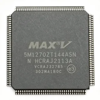
EPF6024ATC144-23 - FLEX 6000 FPGA, 24K Gates, 117 I/O | Altera
MPN: EPF6024ATC144-23 ✗ End of Life| Qty | Unit Price | Extended |
|---|---|---|
| 1 | $18.5 | $18.50 |
| 10 | $16.2 | $162.00 |
| 100 | $13.95 | $1,395.00 |
| 500 | $11.4 | $5,700.00 |
| 1,000 | $9.85 | $9,850.00 |
EPF6024ATC144-23 Overview
A Field Programmable Gate Array (FPGA) is a type of programmable logic device (PLD) that combines the density of a gate array with the in-system reprogrammability of a logic device. FPGAs sit at the top of the programmable logic hierarchy: PLD -> CPLD -> FPGA, and are widely used as flexible alternatives to fixed gate-array ASICs during prototyping and in low-to-medium volume production. The FLEX 6000 family specifically targets low-cost, high-volume designs where fast design changes are required without the NRE costs of mask-programmed logic.
The EPF6024ATC144-23 features a continuous, hierarchical routing architecture with carry chains for high-speed arithmetic and cascade chains for wide-input functions, both of which connect Logic Elements (LEs) within and across LABs. The IC supports in-system configuration via the Altera (now Intel) MAX+PLUS II or Quartus design environment, allowing engineers to iterate quickly on glue logic, bus interfaces, and state-machine controllers. Its 117 available I/Os make it suitable for bridging multiple peripheral buses in cost-sensitive embedded designs.
Typical applications include telecommunications glue logic, industrial control and instrumentation front-ends, peripheral bus bridges (e.g., UART, SPI, or I2C controllers), and prototype replacement of small ASICs. The wide 5.0 V I/O tolerance (with appropriate pull-up design) also simplifies interfacing to legacy 5.0 V peripherals in retrofit designs. Designers migrating from older discrete-logic implementations typically select the EPF6024ATC144 family to consolidate board real-estate while maintaining 5.0 V compatibility.
When designing with this device, attention must be paid to the I/O bank's VCCIO supply voltage - the part supports 3.3 V CMOS outputs natively, but 5.0 V CMOS input thresholds require external pull-up resistors as detailed in the FLEX 6000 datasheet family. Configuration storage is volatile (SRAM-based), so the bitstream must be reloaded from a boot PROM on every power-up. Designers should also verify the exact speed grade (-1, -2, -3) needed for their timing budget; the -23 suffix indicates a specific speed grade and temperature range combination that should be matched against timing-closure requirements before PCB commit.
Drop-in alternatives for EPF6024ATC144-23 — same package, pin-to-pin compatible. Different-package parts requiring PCB rework are excluded.
Variants in this series
Same-series models that are drop-in compatible with EPF6024ATC144-23 (same form factor and footprint) — differing in Package, Speed Grade, Process Technology, Configuration Memory, Operating Temperature.
Quick Comparison Tool — Select alternative parts for side-by-side comparison:
EPF6024ATC144-3
✅ Drop-In✓ In Stock
$14.1 / Unit
View Datasheet →EPF6024ATC144-3N
✅ Drop-In✓ In Stock
$21.4 / Unit
View Datasheet →EPF6024ATC144-2N
✅ Drop-In✓ In Stock
$20.95 / Unit
View Datasheet →EPF6024ATC144-1N
✅ Drop-In✓ In Stock
$20.95 / Unit
View Datasheet →EPF6024ATC144-10
✅ Drop-In✓ In Stock
$11.1 / Unit
View Datasheet →EPF6024ATC144-20
✅ Drop-In✓ In Stock
$9.95 / Unit
View Datasheet →EPF6024ATC144-23 Maximum Ratings & Electrical Characteristics
| Device Family | FLEX 6000 |
| Series | EPF6024 |
| Typical Gates | 24,000 |
| Logic Elements | 1,960 |
| Logic Array Blocks (LABs) | 196 |
| User I/O Pins | 117 |
| Process Technology | 0.42 um CMOS, SRAM-based |
| Maximum Internal Frequency | 142.86 MHz |
| Core Supply Voltage (VCCINT) | 3.3 V |
| I/O Supply Voltage (VCCIO) | 3.3 V (5.0 V tolerant with pull-up) |
| Package | TQFP-144 |
| Pin Count | 144 |
| Mounting Type | Surface Mount |
| Speed Grade | -23 (combined speed/temperature suffix) |
| Configuration Memory | Volatile SRAM (requires boot device) |
EPF6024ATC144-23 tqfp-144 Pin Configuration Guide
Pin configuration for EPF6024ATC144-23 (tqfp-144 package). This digital IC includes GPIO, communication interfaces (UART, SPI, I2C), and power pins. Refer to the manufacturer datasheet for alternate pin functions and configuration options. Essential for embedded system design and PCB layout.

No detailed pinout data available for EPF6024ATC144-23.
Refer to the datasheet for full pin configuration.
Typical Applications
EPF6024ATC144-23 is suitable for 6 applications: Telecommunications Glue Logic, Industrial Control Front-End, Peripheral Bus Bridge, ASIC Prototype Replacement, Legacy 5.0 V System Integration, Test & Measurement Custom Logic.
Telecommunications Glue Logic
The EPF6024ATC144-23 fits telecommunications glue-logic designs thanks to its 1,960 logic elements, 196 LABs, and 117 user I/Os - enough to implement multiple bus bridges, FIFOs, and protocol converters in a single chip. Placed between a microcontroller and legacy telecom peripherals, the FPGA absorbs timing-sensitive glue that would otherwise require a handful of 74-series discrete logic chips, reducing board area and BOM count. With 142.86 MHz internal frequency and 3.3 V core, it handles E1/T1 framing, UART multiplexing, and HDLC-style controllers comfortably. Compared to discrete logic, designers gain in-system reprogrammability for last-minute protocol changes without board rework.
Recommended
Industrial Control Front-End
In industrial control front-ends the EPF6024ATC144-23 serves as a programmable I/O expander and signal-conditioning controller, mapping 117 I/O pins to sensors, optocouplers, and motor-driver enable lines. Its 5.0 V tolerant I/O (with pull-up) simplifies interfacing to legacy industrial sensors running at 5 V logic, while the 3.3 V core keeps power dissipation manageable. The FPGA can implement encoder decoding, PWM generation, and watchdog logic for PLC-style systems, replacing several PAL/GAL devices with one reprogrammable part. Designers value the in-system upgrade path for fixing field bugs without board swap.
Recommended
Peripheral Bus Bridge
The EPF6024ATC144-23 is well matched to bus-bridge applications where mismatched peripheral buses (e.g., 8-bit legacy MCU bus to 16-bit or 32-bit host) must be reconciled. Its 117 I/Os comfortably absorb 32-bit datapath plus control signals, and the carry-chain / cascade-chain architecture accelerates address decoding and wait-state generation. Designers typically instantiate custom state machines to translate handshakes between asynchronous buses with deterministic latency. The SRAM-based configuration allows field upgrades when a new peripheral is added, without respinning the host board.
Recommended
ASIC Prototype Replacement
The EPF6024ATC144-23 functions as an ASIC prototype replacement for low-volume or pre-mask designs, letting engineers validate logic and timing in silicon before committing to a gate-array NRE. With 24K typical gates it captures small to medium fixed-logic designs, and the FLEX 6000 routing fabric closely approximates gate-array timing for honest pre-silicon validation. Designers can iterate on RTL each night and reconfigure the FPGA the next morning, compressing prototype cycles from weeks to days. Once the design stabilizes, the FPGA bitstream is replaced by a mask-programmed gate array with equivalent footprint.
Recommended
Legacy 5.0 V System Integration
Retrofit and brownfield designs benefit from the EPF6024ATC144-23's 5.0 V tolerant I/O capability, which lets the 3.3 V core FPGA directly interface to legacy 5.0 V peripherals using the datasheet-specified pull-up resistor network. Designers use it to modernize older boards by adding programmable logic without redesigning the surrounding 5.0 V analog and digital circuitry. The 144-pin TQFP package footprint matches that of many legacy FPGAs and ASICs, simplifying PCB reuse during technology refresh projects where the host board must remain untouched.
Recommended
Test & Measurement Custom Logic
In bench-top test and measurement instruments the EPF6024ATC144-23 implements custom timing generators, pattern generators, and protocol analyzers that do not exist as off-the-shelf ICs. Engineers exploit the 117 I/Os and 142.86 MHz internal frequency to build stimulus-response capture systems, parallel pattern comparators, and timing-edge counters. The SRAM-based configuration lets test engineers evolve the stimulus patterns between calibration cycles without board changes. Compared to discrete TTL test fixtures, the FPGA consolidates a rack of programmable pulse generators into a single chip.
Recommended
Recommended Products Summary
Engineering reference data for EPF6024ATC144-23 — comparison, design guidance, and compliance information.
Selection Guide
Comparison with Alternatives
| Parameter | This Product | EPF6024ATC144-3 | EPF6024ATC144-3N | EPF6024ATC144-2N |
|---|---|---|---|---|
| Brand | Altera (Intel) | Altera (Intel) | Altera (Intel) | Altera (Intel) |
| Package | TQFP-144 | TQFP-144 - same | TQFP-144 - same | TQFP-144 - same |
| Typical Gates | 24,000 | 24,000 | 24,000 | 24,000 |
| Logic Elements | 1,960 | 1,960 | 1,960 | 1,960 |
| User I/Os | 117 | 117 | 117 | 117 |
| Speed Grade | -23 | -3 (faster) | -3N (faster, lead-free) | -2N (slower, industrial) |
| Core Voltage | 3.3 V | 3.3 V | 3.3 V | 3.3 V |
| Lifecycle Status | Obsolete | Obsolete | Obsolete | Obsolete |
Key Differentiators
- Same TQFP-144 footprint across the entire EPF6024ATC144 family (vs EPF6016ATC144-3)
- Wide 5.0 V tolerant I/O simplifies legacy interfacing (vs EPF6024ATC144-3)
- Speed-grade flexibility within the same silicon (vs EPF6024ATC144-1N)
Design Notes
Estimated: at 100% toggle rate with all 117 I/Os switching, ICCINT current is approximately 30-50 mA per Altera FLEX 6000 datasheet family guidance, giving 3.3 V × 0.05 A ≈ 0.165 W core dissipation. Add 5-10 mA per toggling I/O for VCCIO supply current. Designers should provide local 0.1 uF + 10 uF bulk decoupling on every VCCINT and VCCIO pin to suppress switching transients in the 3.3 V rail.
Because the FLEX 6000 uses SRAM-based configuration, the bitstream is lost on every power-down. A serial configuration PROM (e.g., EPC1064 or EPC1441) must be present on the board, and CONF_DONE must be monitored in firmware to confirm successful configuration before releasing system resets. Designs that omit the boot PROM will fail silently with the FPGA in undefined state - this is the most common support issue when maintaining legacy boards.
The TQFP-144 package has 0.5 mm pitch leads that require careful PCB layout - keep ground plane continuous under the package, use micro-vias or dogbone fan-outs for inner-row pads, and reserve at least 4 layers (signal, ground, power, signal) for noise-sensitive designs. Place configuration clock (DCLK) traces short and away from switching outputs to avoid bitstream corruption during multi-device JTAG chains. JTAG pins (TCK, TMS, TDI, TDO) need 4.7 kohm pull-ups per IEEE 1149.1.
Compliance Information
RoHS/REACH compliance for EPF6024ATC144-23 is not documented in current distributor listings because the FLEX 6000 family is obsolete. The -3N and -2N suffixes in the family are marketed as lead-free variants. AEC-Q100 is not applicable - FPGAs are not automotive-qualified in this family.