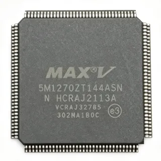
EPF6024ATI144-1 - FLEX 6000 FPGA 24K Gates | Altera | TQFP-144
MPN: EPF6024ATI144-1 ✗ End of Life| Qty | Unit Price | Extended |
|---|---|---|
| 1 | $45 | $45.00 |
| 10 | $40.5 | $405.00 |
| 100 | $36 | $3,600.00 |
| 500 | $32.5 | $16,250.00 |
| 1,000 | $28.8 | $28,800.00 |
EPF6024ATI144-1 Overview
An FPGA (Field-Programmable Gate Array) is a programmable logic device that lets designers implement arbitrary digital logic in a single IC. FPGAs sit between simple PLDs and full ASICs in the logic-device hierarchy, offering higher density than CPLDs and lower NRE cost than ASICs. The FLEX 6000 family specifically targets glue-logic and bus-interface applications where density, low cost, and SRAM-based reconfigurability matter more than high-speed transceivers or block RAM.
Key features of the EPF6024ATI144-1 include 24,000 typical gates (16,000 usable), 1960 logic elements (LEs), 117,000 bits of RAM, and 117 I/O pins across 8 I/O banks. Maximum operating frequency is rated at 172 MHz, and the device operates from a 3.3 V core supply. The part is specified for the industrial temperature range (-40C to +85C), making it suitable for moderate-environment industrial, telecom, and embedded-control applications.
The FLEX 6000 architecture combines fine-grained logic elements with a continuous FastTrack interconnect, providing predictable interconnect delays independent of logic placement. Each LE contains a 4-input look-up table (LUT), a programmable register, and dedicated carry and cascade chains. Configuration is stored in SRAM, requiring a configuration device such as the EPC2 or EPC8 at power-up.
Typical applications include industrial control and factory automation glue logic, telecommunications line-card interfaces, networking glue and protocol bridging, printer and image-processing controllers, and legacy PCI/ISA bus-interface designs. The wide I/O count (117 pins) and 3.3 V operation make it a drop-in replacement for older FLEX 6000 designs during board revision.
When designing with this part, ensure the board provides a configuration device (EPC2/EPC8) or microprocessor pull-up for SRAM-based configuration. The TQFP-144 footprint requires a 4-layer PCB minimum for signal integrity at 172 MHz. Note that FLEX 6000 is now a legacy part, so long-term availability planning is recommended.
This page synthesizes distributor stock data, same-family drop-in alternatives, and practical FLEX 6000 design notes not found in the standalone Altera datasheet.
Drop-in alternatives for EPF6024ATI144-1 — same package, pin-to-pin compatible. Different-package parts requiring PCB rework are excluded.
Variants in this series
Same-series models that are drop-in compatible with EPF6024ATI144-1 (same form factor and footprint) — differing in Package, Process Technology, Operating Temperature, RoHS Status, Speed Grade.
Quick Comparison Tool — Select alternative parts for side-by-side comparison:
EPF6024ATC144-1
✅ Drop-In✓ In Stock
$8.2 / Unit
View Datasheet →EPF6024ATC144-2
✅ Drop-In✓ In Stock
$24.95 / Unit
View Datasheet →EPF6024ATC144-3
✅ Drop-In✓ In Stock
$14.1 / Unit
View Datasheet →EPF6016ATI144-3
✅ Drop-In✓ In Stock
$15.9 / Unit
View Datasheet →EPF6016ATI144-2
✅ Drop-In✓ In Stock
$9.4 / Unit
View Datasheet →EPF6024ATI144-1 Maximum Ratings & Electrical Characteristics
| Family | FLEX 6000 |
| Series | EPF6024A |
| Typical Gates | 24,000 |
| Usable Gates | 16,000 |
| Logic Elements (LEs) | 1,960 |
| Embedded RAM Bits | 117,000 bits |
| Maximum User I/O Pins | 117 |
| I/O Banks | 8 |
| Core Voltage | 3.3 V |
| Maximum Operating Frequency | 172 MHz |
| Process Technology | CMOS SRAM |
| Package | TQFP-144 |
| Terminal Pitch | 0.5 mm |
| Package Height | 1.6 mm |
| Operating Temperature Range | -40C to +85C (Industrial) |
| Mounting Type | Surface Mount |
| RoHS Status | Non-RoHS Compliant |
EPF6024ATI144-1 1.6 mm Pin Configuration Guide
Pin configuration for EPF6024ATI144-1 (1.6 mm package). This digital IC includes GPIO, communication interfaces (UART, SPI, I2C), and power pins. Refer to the manufacturer datasheet for alternate pin functions and configuration options. Essential for embedded system design and PCB layout.

No detailed pinout data available for EPF6024ATI144-1.
Refer to the datasheet for full pin configuration.
Typical Applications
EPF6024ATI144-1 is suitable for 7 applications: Industrial Glue Logic Replacement, Telecommunications Line-Card Interface, Legacy PCI / ISA Bus Bridge, Printer and Image-Processing Controller, Embedded Control and HMI Logic, Networking Protocol Bridging, Test and Measurement Front-End Logic.
Industrial Glue Logic Replacement
The EPF6024ATI144-1 fits industrial glue-logic replacement because its 1,960 logic elements and 117 I/O pins provide ample capacity to absorb dozens of 74-series TTL parts on legacy factory-control boards. Its industrial temperature rating (-40C to +85C) matches the thermal envelope of PLC backplanes and motor-drive controllers, while the 3.3 V core supply simplifies power-tree design on retrofits. The 172 MHz fMAX comfortably handles typical glue-logic functions like address decoding, bus multiplexing, and state-machine sequencing. Replacing discrete logic with the EPF6024ATI144-1 cuts board area and BOM cost while preserving the original schematic intent.
Recommended
Telecommunications Line-Card Interface
The EPF6024ATI144-1 suits telecommunications line-card interface logic because its 117 I/O pins easily accommodate parallel TDM bus glue, framing logic, and clock-distribution functions on legacy T1/E1 line cards. The 8 I/O banks support mixed-voltage interfacing (3.3 V, 2.5 V, 1.8 V) required when bridging legacy framers with newer PHY ICs. The 172 MHz internal performance handles HDLC controllers and channel-associated signalling at full rate. SRAM-based reconfigurability allows field-upgrading of line-card firmware without replacing the hardware.
Recommended
Legacy PCI / ISA Bus Bridge
The EPF6024ATI144-1 is well-suited to legacy PCI and ISA bus bridge applications because its 3.3 V I/O compliance and 117 user pins provide the necessary fan-out for 32-bit bus multiplexing, address decoding, and wait-state insertion. PCI 33 MHz clocking (33 MHz bus) fits well within the 172 MHz internal fMAX, leaving headroom for bus-turnaround and parity-generation logic. The TQFP-144 footprint is large enough to break out all PCI control signals plus interrupt and arbitration glue. Designers maintaining legacy industrial PCs continue to use this part as a bridge to modern PCIe hosts via external controller chips.
Recommended
Printer and Image-Processing Controller
The EPF6024ATI144-1 serves printer and image-processing controllers well because its 1,960 logic elements can implement DMA engines, video-data packers/unpackers, and engine-control state machines in a single device. The 117 I/O pins accept parallel sensor interfaces from CCD/CMOS line scanners and drive print-engine stepper controllers simultaneously. Internal RAM (117 Kbits) supports small line buffers and LUT-based gamma correction. The SRAM reconfigurability is useful for OEM firmware variants (different printer models) sharing the same controller PCB.
Recommended
Embedded Control and HMI Logic
The EPF6024ATI144-1 fits embedded control and human-machine interface (HMI) logic because it can integrate display multiplexers, keypad scanners, PWM generators, and serial-bus bridges (UART/SPI/I2C) in a single chip. Its industrial temperature rating supports factory-floor HMIs and outdoor kiosks. The 172 MHz performance handles real-time control loops and display-refresh DMA without external microsequencer support. Designers often pair this part with a low-cost microcontroller for task partitioning: MCU handles protocol stack, FPGA handles deterministic I/O.
Recommended
Networking Protocol Bridging
The EPF6024ATI144-1 works well in networking protocol bridging applications because it can implement framers, MAC-layer glue, and traffic-shaping FIFOs alongside off-the-shelf PHY and switch ICs. The 8 I/O banks allow direct interfacing between 3.3 V Ethernet MACs and 1.8 V SERDES devices on the same board. SRAM reconfigurability supports multi-protocol line cards (e.g., Ethernet-to-SONET bridging) where one hardware platform serves multiple standards via firmware. The 117 I/O count and 1,960 LEs comfortably absorb bridging logic plus statistics counters.
Recommended
Test and Measurement Front-End Logic
The EPF6024ATI144-1 suits test and measurement front-end logic because it can implement pattern generators, signal-routing matrices, and timing/sequencer blocks for ATE and bench instruments. The 117 I/O pins allow direct interfacing with parallel DAC/ADC front-ends, while the 172 MHz internal performance supports pattern rates into the tens of MHz. SRAM reconfigurability lets the same instrument hardware serve multiple DUT families by loading different test personalities. Industrial temperature rating supports lab-to-factory portability.
Recommended
Recommended Products Summary
Engineering reference data for EPF6024ATI144-1 — comparison, design guidance, and compliance information.
Selection Guide
Comparison with Alternatives
| Parameter | This Product | EPF6024ATC144-1 | EPF6024ATC144-2 | EPF6024ATC144-3 | EPF6016ATI144-3 | EPF6016ATI144-2 |
|---|---|---|---|---|---|---|
| Package | TQFP-144 | TQFP-144 - same | TQFP-144 - same | TQFP-144 - same | TQFP-144 - same | TQFP-144 - same |
| Brand | Altera | Altera | Altera | Altera | Altera | Altera |
| Typical Gates | 24,000 | 24,000 | 24,000 | 24,000 | 16,000 (-33%) | 16,000 (-33%) |
| Logic Elements | 1,960 | 1,960 | 1,960 | 1,960 | 1,320 (-33%) | 1,320 (-33%) |
| User I/O Pins | 117 | 117 | 117 | 117 | 117 | 117 |
| Operating Temperature | -40C to +85C (Industrial) | 0C to +70C (Commercial) | 0C to +70C (Commercial) | 0C to +70C (Commercial) | -40C to +85C (Industrial) | -40C to +85C (Industrial) |
| Core Voltage | 3.3 V | 3.3 V | 3.3 V | 3.3 V | 3.3 V | 3.3 V |
| RoHS Compliance | Non-RoHS | Non-RoHS | RoHS (likely reflow variant) | RoHS (likely reflow variant) | Non-RoHS | RoHS (likely reflow variant) |
Key Differentiators
- Industrial temperature range with same TQFP-144 footprint (vs EPF6024ATC144-1)
- Higher logic density vs. EPF6016 family (vs EPF6016ATI144-3)
- Same-density, commercial-temperature drop-in for indoor designs (vs EPF6024ATC144-2)
Design Notes
The EPF6024ATI144-1 requires a stable 3.3 V VCCINT supply with separate VCCIO pins per I/O bank. Estimated: at 100% toggle rate and 117 active outputs, ICCINT draws approximately 200-400 mA, requiring a 1 A regulator with 100 mV tolerance. Add 10 uF bulk + 0.1 uF decoupling per VCC pin, placed within 5 mm of the package. Power sequencing must keep VCCINT within 2.0 V of VCCIO during ramp to prevent I/O latch-up. For battery-backed SRAM configuration retention, hold nCONFIG low during power transitions.
TQFP-144 with 0.5 mm pitch requires a 4-layer PCB with continuous ground plane beneath the device. Estimated: route all signal traces on outer layers with 0.2 mm width and 0.15 mm clearance; inner layers reserved for power and ground. Use microvia or dog-bone fanout for the 117 I/O pins to inner breakout rows. Maintain 50 ohm controlled impedance for clocks and JTAG signals. Place the configuration PROM (EPC2/EPC8) within 50 mm to minimize DCLK/DATA0 trace length and avoid reflection-induced configuration failures.
Common pitfalls: (1) Forgetting the external pull-up on nCONFIG - if left floating, the device may enter undefined configuration state; (2) Using TC (commercial) variants instead of TI (industrial) in factory-floor designs - commercial parts fail at temperatures below 0C; (3) Assuming the TQFP-144 footprint matches PQFP-208 - the 208-pin variants have different pin assignments and cannot be drop-in swapped; (4) Skipping JTAG boundary-scan testing - FLEX 6000 supports IEEE 1149.1, so use it during prototype bring-up; (5) Not validating configuration PROM image compatibility when migrating between speed grades (-1, -2, -3).
The TQFP-144 package has a thermal resistance of approximately 35-40 C/W theta-JA on a 4-layer PCB. Estimated: at full I/O toggle and 3.3 V core, junction-to-ambient rise is 15-25C. For industrial temperature operation up to +85C ambient, total power dissipation must stay below 1 W for adequate margin. Add thermal vias beneath the exposed die-attach pad (if present) and connect them to the ground plane. Forced airflow is recommended for high-density designs with sustained 172 MHz operation.
Compliance Information
Marked as Non-RoHS Compliant in distributor listings. Original FLEX 6000 family parts predate full RoHS transition. Lead-bearing TQFP-144 package. REACH, halogen-free, and conflict-minerals status not documented in available distributor data.