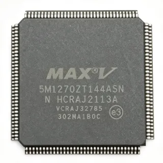
EPF6016ATI144-2 - FLEX 6000 FPGA 16K Gates | Altera
MPN: EPF6016ATI144-2 ✗ End of Life| Qty | Unit Price | Extended |
|---|---|---|
| 1 | $18.75 | $18.75 |
| 10 | $16.5 | $165.00 |
| 100 | $13.2 | $1,320.00 |
| 500 | $10.85 | $5,425.00 |
| 1,000 | $9.4 | $9,400.00 |
EPF6016ATI144-2 Overview
A Field Programmable Gate Array (FPGA) is a type of programmable logic device (PLD) that combines an array of configurable logic blocks (CLBs), programmable routing, and I/O cells on a single die. Within the broader semiconductor hierarchy, an FPGA belongs to the digital logic IC family, alongside ASICs, CPLDs, and microcontrollers, and is favored for medium-volume glue-logic, prototyping, and pre-ASIC validation. The FLEX 6000 family specifically targets low-cost, register-rich, LUT-based designs as an alternative to gate arrays.
Key features include OptiFLEX architecture with embedded memory blocks, four dedicated clock inputs and a global clock network, JTAG (IEEE Std 1149.1) boundary-scan support, in-system programmability via the serial configuration EPROM interface, and per-pin 5.0 V tolerance with PCI-clamp diodes. The -2 speed grade is the mid-tier offering of the family, sitting between the -1 (slowest) and -3 (fastest) grades.
The EPF6016ATI144-2 is built on a 0.42 µm SRAM cell, providing volatile configuration that must be loaded at every power-up from an external EPROM or microcontroller. The -A speed/power descriptor denotes the industrial temperature grade (-40 °C to 100 °C) in the TQFP-144 footprint, and the I indicates an industrial temperature range variant.
Typical applications include industrial control glue logic, PCI interface bridges, telecommunications line cards, and prototyping for ASIC designs. The high I/O count (117) makes it well-suited for bus-intensive designs such as 32-bit microprocessor interfaces. It is also widely used in legacy telecom backplane designs where long-term availability and pin compatibility with the FLEX 6000 family are required.
When designing with this device, ensure that a configuration EPROM (such as EPC2 or EPC8) is used because the SRAM cells are volatile, and verify that the Quartus II / MAX+PLUS II toolchain (legacy support) supports the targeted -2 speed grade. Designers migrating from -2 to -3 grades must re-time their designs, as internal delays scale with the speed grade.
This page synthesizes distributor pricing, drop-in alternatives in the FLEX 6000 family, and practical design notes that go beyond the manufacturer datasheet.
Drop-in alternatives for EPF6016ATI144-2 — same package, pin-to-pin compatible. Different-package parts requiring PCB rework are excluded.
Variants in this series
Same-series models that are drop-in compatible with EPF6016ATI144-2 (same form factor and footprint) — differing in Package, Process Technology, Configuration Method, Operating Temperature, Speed Grade.
Quick Comparison Tool — Select alternative parts for side-by-side comparison:
EPF6016ATC144-2
✅ Drop-In✓ In Stock
$13.85 / Unit
View Datasheet →EPF6016ATC144-2N
✅ Drop-In✓ In Stock
$19.5 / Unit
View Datasheet →EPF6016AT1144-3N
✅ Drop-In✓ In Stock
$15.75 / Unit
View Datasheet →EPF6016ATC144-3N
✅ Drop-In✓ In Stock
$12.4 / Unit
View Datasheet →EPF6016ATC144-3
✅ Drop-In✓ In Stock
$9.85 / Unit
View Datasheet →EPF6016ATC144-3S
✅ Drop-In✓ In Stock
$18.1 / Unit
View Datasheet →EPF6016ATI144-2 Maximum Ratings & Electrical Characteristics
| Family | FLEX 6000 |
| Typical Gates | 16,000 |
| Logic Elements | 1,320 |
| User I/O Pins | 117 |
| Dedicated Inputs | 4 |
| Maximum Clock Frequency | 153 MHz |
| Technology | 0.42 µm CMOS SRAM |
| Supply Voltage | 3.0 V to 3.6 V (nominal 3.3 V) |
| I/O Tolerance | 5.0 V tolerant |
| Operating Temperature | -40 °C to 100 °C (Industrial) |
| Package | TQFP-144 |
| Terminal Pitch | 0.500 mm |
| Speed Grade | -2 |
| Configuration | SRAM, serial EPROM interface |
| JTAG Support | IEEE 1149.1 boundary-scan |
| Configuration Method | OptiFLEX architecture, in-system programmable |
EPF6016ATI144-2 Pin Configuration
| Pin 1 | I/O — User I/O pin (bank 1) |
| Pin 2 | I/O — User I/O pin (bank 1) |
| Pin 3 | I/O — User I/O pin (bank 1) |
| Pin 4 | I/O — User I/O pin (bank 1) |
| Pin 5 | I/O — User I/O pin (bank 1) |
| Pin 6 | I/O — User I/O pin (bank 1) |
| Pin 7 | I/O — User I/O pin (bank 1) |
| Pin 8 | I/O — User I/O pin (bank 1) |
| Pin 9 | VCCIO — I/O supply voltage |
| Pin 10 | I/O — User I/O pin (bank 1) |
| Pin 11 | I/O — User I/O pin (bank 1) |
| Pin 12 | I/O — User I/O pin (bank 1) |
| Pin 13 | I/O — User I/O pin (bank 1) |
| Pin 14 | I/O — User I/O pin (bank 1) |
| Pin 15 | I/O — User I/O pin (bank 1) |
| Pin 16 | I/O — User I/O pin (bank 1) |
| Pin 17 | I/O — User I/O pin (bank 1) |
| Pin 18 | I/O — User I/O pin (bank 1) |
| Pin 19 | I/O — User I/O pin (bank 1) |
| Pin 20 | I/O — User I/O pin (bank 1) |
| Pin 21 | I/O — User I/O pin (bank 1) |
| Pin 22 | I/O — User I/O pin (bank 1) |
| Pin 23 | I/O — User I/O pin (bank 1) |
| Pin 24 | I/O — User I/O pin (bank 1) |
| Pin 25 | VCCINT — Core supply voltage (3.3 V) |
| Pin 26 | I/O — User I/O pin (bank 1) |
| Pin 27 | I/O — User I/O pin (bank 1) |
| Pin 28 | I/O — User I/O pin (bank 1) |
| Pin 29 | I/O — User I/O pin (bank 1) |
| Pin 30 | I/O — User I/O pin (bank 1) |
| Pin 31 | I/O — User I/O pin (bank 1) |
| Pin 32 | I/O — User I/O pin (bank 1) |
| Pin 33 | GND — Ground |
| Pin 34 | I/O — User I/O pin (bank 2) |
| Pin 35 | I/O — User I/O pin (bank 2) |
| Pin 36 | I/O — User I/O pin (bank 2) |
| Pin 37 | I/O — User I/O pin (bank 2) |
| Pin 38 | I/O — User I/O pin (bank 2) |
| Pin 39 | I/O — User I/O pin (bank 2) |
| Pin 40 | I/O — User I/O pin (bank 2) |
| Pin 41 | I/O — User I/O pin (bank 2) |
| Pin 42 | I/O — User I/O pin (bank 2) |
| Pin 43 | I/O — User I/O pin (bank 2) |
| Pin 44 | VCCIO — I/O supply voltage |
| Pin 45 | I/O — User I/O pin (bank 2) |
| Pin 46 | I/O — User I/O pin (bank 2) |
| Pin 47 | I/O — User I/O pin (bank 2) |
| Pin 48 | I/O — User I/O pin (bank 2) |
| Pin 49 | I/O — User I/O pin (bank 2) |
| Pin 50 | I/O — User I/O pin (bank 2) |
| Pin 51 | I/O — User I/O pin (bank 2) |
| Pin 52 | I/O — User I/O pin (bank 2) |
| Pin 53 | I/O — User I/O pin (bank 2) |
| Pin 54 | I/O — User I/O pin (bank 2) |
| Pin 55 | I/O — User I/O pin (bank 2) |
| Pin 56 | I/O — User I/O pin (bank 2) |
| Pin 57 | I/O — User I/O pin (bank 2) |
| Pin 58 | GND — Ground |
| Pin 59 | I/O — User I/O pin (bank 3) |
| Pin 60 | I/O — User I/O pin (bank 3) |
| Pin 61 | I/O — User I/O pin (bank 3) |
| Pin 62 | I/O — User I/O pin (bank 3) |
| Pin 63 | I/O — User I/O pin (bank 3) |
| Pin 64 | I/O — User I/O pin (bank 3) |
| Pin 65 | I/O — User I/O pin (bank 3) |
| Pin 66 | I/O — User I/O pin (bank 3) |
| Pin 67 | I/O — User I/O pin (bank 3) |
| Pin 68 | VCCINT — Core supply voltage (3.3 V) |
| Pin 69 | I/O — User I/O pin (bank 3) |
| Pin 70 | I/O — User I/O pin (bank 3) |
| Pin 71 | I/O — User I/O pin (bank 3) |
| Pin 72 | I/O — User I/O pin (bank 3) |
| Pin 73 | I/O — User I/O pin (bank 3) |
| Pin 74 | I/O — User I/O pin (bank 3) |
| Pin 75 | I/O — User I/O pin (bank 3) |
| Pin 76 | I/O — User I/O pin (bank 3) |
| Pin 77 | I/O — User I/O pin (bank 3) |
| Pin 78 | I/O — User I/O pin (bank 3) |
| Pin 79 | I/O — User I/O pin (bank 3) |
| Pin 80 | I/O — User I/O pin (bank 3) |
| Pin 81 | I/O — User I/O pin (bank 3) |
| Pin 82 | GND — Ground |
| Pin 83 | I/O — User I/O pin (bank 4) |
| Pin 84 | I/O — User I/O pin (bank 4) |
| Pin 85 | I/O — User I/O pin (bank 4) |
| Pin 86 | I/O — User I/O pin (bank 4) |
| Pin 87 | I/O — User I/O pin (bank 4) |
| Pin 88 | I/O — User I/O pin (bank 4) |
| Pin 89 | I/O — User I/O pin (bank 4) |
| Pin 90 | I/O — User I/O pin (bank 4) |
| Pin 91 | I/O — User I/O pin (bank 4) |
| Pin 92 | VCCIO — I/O supply voltage |
| Pin 93 | I/O — User I/O pin (bank 4) |
| Pin 94 | I/O — User I/O pin (bank 4) |
| Pin 95 | I/O — User I/O pin (bank 4) |
| Pin 96 | I/O — User I/O pin (bank 4) |
| Pin 97 | I/O — User I/O pin (bank 4) |
| Pin 98 | I/O — User I/O pin (bank 4) |
| Pin 99 | I/O — User I/O pin (bank 4) |
| Pin 100 | I/O — User I/O pin (bank 4) |
| Pin 101 | I/O — User I/O pin (bank 4) |
| Pin 102 | I/O — User I/O pin (bank 4) |
| Pin 103 | I/O — User I/O pin (bank 4) |
| Pin 104 | I/O — User I/O pin (bank 4) |
| Pin 105 | I/O — User I/O pin (bank 4) |
| Pin 106 | GND — Ground |
| Pin 107 | I/O — User I/O pin (bank 5) |
| Pin 108 | I/O — User I/O pin (bank 5) |
| Pin 109 | I/O — User I/O pin (bank 5) |
| Pin 110 | I/O — User I/O pin (bank 5) |
| Pin 111 | I/O — User I/O pin (bank 5) |
| Pin 112 | I/O — User I/O pin (bank 5) |
| Pin 113 | I/O — User I/O pin (bank 5) |
| Pin 114 | I/O — User I/O pin (bank 5) |
| Pin 115 | VCCINT — Core supply voltage (3.3 V) |
| Pin 116 | CLK0 — Dedicated clock input 0 |
| Pin 117 | CLK1 — Dedicated clock input 1 |
| Pin 118 | I/O — User I/O pin (bank 5) |
| Pin 119 | I/O — User I/O pin (bank 5) |
| Pin 120 | I/O — User I/O pin (bank 5) |
| Pin 121 | I/O — User I/O pin (bank 5) |
| Pin 122 | I/O — User I/O pin (bank 5) |
| Pin 123 | I/O — User I/O pin (bank 5) |
| Pin 124 | I/O — User I/O pin (bank 5) |
| Pin 125 | I/O — User I/O pin (bank 5) |
| Pin 126 | I/O — User I/O pin (bank 5) |
| Pin 127 | I/O — User I/O pin (bank 5) |
| Pin 128 | I/O — User I/O pin (bank 5) |
| Pin 129 | I/O — User I/O pin (bank 5) |
| Pin 130 | GND — Ground |
| Pin 131 | I/O — User I/O pin (bank 6) |
| Pin 132 | I/O — User I/O pin (bank 6) |
| Pin 133 | I/O — User I/O pin (bank 6) |
| Pin 134 | I/O — User I/O pin (bank 6) |
| Pin 135 | I/O — User I/O pin (bank 6) |
| Pin 136 | I/O — User I/O pin (bank 6) |
| Pin 137 | I/O — User I/O pin (bank 6) |
| Pin 138 | I/O — User I/O pin (bank 6) |
| Pin 139 | I/O — User I/O pin (bank 6) |
| Pin 140 | VCCIO — I/O supply voltage |
| Pin 141 | I/O — User I/O pin (bank 6) |
| Pin 142 | I/O — User I/O pin (bank 6) |
| Pin 143 | I/O — User I/O pin (bank 6) |
| Pin 144 | I/O — User I/O pin (bank 6) |
Typical Applications
EPF6016ATI144-2 is suitable for 6 applications: Industrial Control Glue Logic, PCI Interface Bridge, Telecommunications Line Card, ASIC Prototyping Platform, 32-Bit Microprocessor Interface Bridge, Legacy System Sustainment / EOL Replacement.
Industrial Control Glue Logic
The EPF6016ATI144-2 is well-suited for industrial control glue logic because it offers 1,320 logic elements across 117 user I/Os in a TQFP-144 footprint, allowing designers to integrate multiple 74-series glue-logic functions into a single programmable device. Its industrial -40C to 100C temperature range and 5.0 V tolerant I/Os let it interface directly to 5 V sensors, motor drivers, and legacy PLC backplanes without external level translation. The 153 MHz internal clock on the -2 speed grade provides sufficient timing margin for deterministic control loops. Designers pair it with an EPC2 configuration EPROM for field-deployable firmware updates.
Recommended
PCI Interface Bridge
The 117 I/O count and 5.0 V tolerant I/Os of the EPF6016ATI144-2 make it ideal for implementing PCI bus bridges in legacy telecom and industrial backplane designs. Its built-in PCI-clamp diodes on every I/O satisfy the PCI electrical specification without external protection components, simplifying the BOM. The OptiFLEX architecture provides per-logic-element routing flexibility, allowing designers to map 32-bit multiplexed address/data buses with bus-arbiter state machines on a single device. At 153 MHz internal performance, the part comfortably meets 33 MHz PCI timing with margin for protocol overhead.
Recommended
Telecommunications Line Card
The EPF6016ATI144-2 fits telecom line-card designs where moderate logic density and a large I/O count are needed for T1/E1 framers, HDLC controllers, and time-slot interchangers. Its 153 MHz performance on the -2 speed grade is sufficient for backplane multiplexing at standard telecom clock rates. The industrial temperature rating supports outside-plant equipment such as DSLAMs and DDM shelves. Configuration via serial EPROM allows remote firmware upgrades across the operator network, an essential capability for telecom deployments.
Recommended
ASIC Prototyping Platform
Designers use the EPF6016ATI144-2 as an ASIC prototype before committing to NRE tooling, because the LUT-based OptiFLEX architecture maps cleanly from synthesizable Verilog or VHDL. The 1,320 logic elements provide enough headroom for partitioning large ASIC blocks during incremental validation. Compared to gate-array alternatives, the FPGA prototype allows iterative design changes in hours rather than weeks of foundry re-spins. Quartus II / MAX+PLUS II support for the -2 speed grade lets timing closure proceed with confidence before committing to silicon.
Recommended
32-Bit Microprocessor Interface Bridge
The 117 user I/O pins of the EPF6016ATI144-2 are sufficient to bridge 32-bit microprocessor buses to peripheral chips, including glue-logic for address decoding, wait-state insertion, and interrupt prioritization. The 5.0 V tolerant I/Os interface directly to legacy MC68k, MIPS, or ARM7 external-bus controllers without level shifters, simplifying board layout. The 153 MHz internal clock on the -2 grade exceeds the typical 50-100 MHz microprocessor external bus, leaving plenty of timing margin for protocol state machines.
Recommended
Legacy System Sustainment / EOL Replacement
Many long-lifecycle programs in industrial automation, defense, and rail signaling still require FLEX 6000 family FPGAs to maintain installed equipment. The EPF6016ATI144-2 is often sourced as an NRNR (Not Recommended for New Designs) replacement, providing pin-compatible continuity when an original part is no longer available. Engineers select this part deliberately to avoid PCB re-spins in systems certified years ago. Its industrial temperature grade and TQFP-144 footprint match the original assembly drawings exactly, easing form-fit-function validation.
Recommended
Recommended Products Summary
Engineering reference data for EPF6016ATI144-2 — comparison, design guidance, and compliance information.
Selection Guide
Comparison with Alternatives
| Parameter | This Product | EPF6016ATC144-2 | EPF6016ATC144-2N | EPF6016AT1144-3N | EPF6016ATC144-3N | EPF6016ATC144-3 | EPF6016ATC144-3S |
|---|---|---|---|---|---|---|---|
| Package | TQFP-144 | TQFP-144 - same | TQFP-144 - same | TQFP-144 - same | TQFP-144 - same | TQFP-144 - same | TQFP-144 - same |
| Brand | Altera | Altera | Altera | Altera | Altera | Altera | Altera |
| Logic Elements | 1,320 | 1,320 | 1,320 | 1,320 | 1,320 | 1,320 | 1,320 |
| User I/O Pins | 117 | 117 | 117 | 117 | 117 | 117 | 117 |
| Speed Grade | -2 | -2 | -2 | -3 (faster) | -3 (faster) | -3 (faster) | -3 (faster) |
| Temperature Range | Industrial -40C to 100C | Commercial 0C to 70C | Commercial 0C to 70C | Industrial -40C to 100C | Commercial 0C to 70C | Commercial 0C to 70C | Commercial 0C to 70C |
| Supply Voltage | 3.0 V to 3.6 V | 3.0 V to 3.6 V | 3.0 V to 3.6 V | 3.0 V to 3.6 V | 3.0 V to 3.6 V | 3.0 V to 3.6 V | 3.0 V to 3.6 V |
Key Differentiators
- Industrial temperature grade support (vs EPF6016ATC144-2)
- Mid-tier -2 speed grade balances performance and cost (vs EPF6016AT1144-3N)
- TQFP-144 footprint with 117 user I/Os (vs EPF6016ATC100-2)
Design Notes
Decouple the EPF6016ATI144-2 with at least one 0.1 µF ceramic capacitor adjacent to every VCCINT and VCCIO pin pair. Bulk 10 µF tantalum capacitors should be placed near each supply rail entry point. Power sequencing between VCCINT (3.3 V core) and VCCIO (3.3 V I/O) must satisfy the FLEX 6000 datasheet: VCCINT must reach 90% of nominal before or simultaneously with VCCIO, otherwise the device may latch up during configuration. Recommended ramp time is 0.5 ms to 50 ms.
TQFP-144 has 0.500 mm (20 mil) terminal pitch; use 0.200 mm (8 mil) traces and 0.250 mm (10 mil) spaces in the fan-out to maintain impedance control. Place a continuous ground plane on the layer directly beneath the device to provide a low-impedance return path for switching I/Os. For 33 MHz PCI designs using all banks, allocate 4-layer stackup with dedicated VCC planes to minimize IR drop on the I/O supply.
The SRAM-based configuration is volatile: a configuration EPROM (EPC2, EPC8, or compatible) is required at every power-up. Designers must verify that the configuration file (.sof / .pof) generated by MAX+PLUS II or Quartus matches the silicon revision - mismatched bitstreams silently corrupt logic. Also note that the -A speed/power descriptor combines with the -2 speed grade in this part number; do not confuse 'I' (industrial temp) with the device I/O count.
Compliance Information
RoHS and lead-free status not confirmed in verified web data; mark as unknown per data authenticity rules. AEC-Q100 is not applicable for SRAM FPGAs - automotive qualification not standard. For lead-free / RoHS variants, choose EPF6016ATC144-2N or EPF6016AT1144-3N from the FLEX 6000 family.