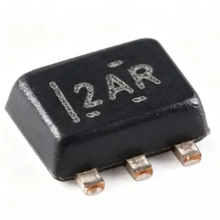
ESD9B3.3ST5G - Bidirectional ESD TVS Diode 3.3V SOD-923 | onsemi
MPN: ESD9B3.3ST5G ✓ Active| Qty | Unit Price | Extended |
|---|---|---|
| 1 | $0.05 | $0.05 |
| 10 | $0.032 | $0.32 |
| 100 | $0.021 | $2.10 |
| 500 | $0.017 | $8.50 |
| 1,000 | $0.0139 | $13.90 |
ESD9B3.3ST5G Overview
A TVS diode is a type of clamp circuit protection device in the broader family of transient voltage suppressors and surge protection components. Placed in parallel with a sensitive signal or power line, it remains high-impedance during normal operation and conducts within nanoseconds when an ESD or surge transient exceeds its breakdown voltage, diverting the surge energy to ground and clamping the line voltage to a safe level.
The ESD9B Series is designed to protect voltage-sensitive components from ESD. According to the onsemi ESD9B datasheet, the series offers excellent clamping capability, low leakage, and fast response time for best-in-class protection on designs exposed to ESD events. The bidirectional 3.3 V configuration supports symmetric positive and negative transient clamping on lines operating up to 3.3 V rails, with IEC 61000-4-2 style ESD robustness of plus or minus 18 kV (air and contact) as reported by distributor listings.
Architecturally, the device uses a silicon avalanche breakdown structure that requires no external drive, no control logic, and no supply rail, making it a zero-quiescent-current protection element. Its micro-packaged SOD-923 footprint minimizes loop inductance, which directly improves clamping performance on fast-rise-time ESD waveforms; shorter loop inductance equals lower residual clamped voltage at the protected IC.
Typical applications include cellular phones, MP3 players, digital cameras, tablets, and other portable electronics where board space comes at a premium. The ESD9B3.3ST5G is commonly placed on USB data lines, button/keypad inputs, audio jack lines, GPIO pins, and antenna-fed RF lines running from 3.3 V or lower rails.
Design consideration: place the TVS as close as possible to the connector or entry point and route to a low-impedance ground stitch; the series inductance of a long trace will dominate the residual clamp voltage during a nanosecond ESD pulse.
This page synthesizes verified distributor data, pricing tiers, drop-in alternatives, and practical ESD layout design notes not found in the manufacturer datasheet, providing selection guidance for engineers choosing between 3.3 V and 5 V bidirectional micro-packaged TVS options.
Drop-in alternatives for ESD9B3.3ST5G — same package, pin-to-pin compatible. Different-package parts requiring PCB rework are excluded.
Variants in this series
Same-series models that are drop-in compatible with ESD9B3.3ST5G (same form factor and footprint) — differing in Configuration, Package, Peak Pulse Current (Ipp), Polarity.
Quick Comparison Tool — Select alternative parts for side-by-side comparison:
SZESD9B3.3ST5G
✅ Drop-In📋 Reference alternative (not in catalog)
ESD9X3.3ST5G
✅ Drop-In📋 Reference alternative (not in catalog)
ESD9B5.0ST5G
✅ Drop-In📋 Reference alternative (not in catalog)
ESD9X5.0ST5G
✅ Drop-In✓ In Stock
$0.018 / Unit
View Datasheet →ESD9B3.3ST5G Maximum Ratings & Electrical Characteristics
| Direction | Bidirectional |
| Reverse Working Voltage (VRWM) | 3.3 V |
| Clamping Voltage (Vc max) | 11.5 V |
| Peak Pulse Current (Ipp) | 2 A (8/20 us) |
| ESD Withstand (IEC 61000-4-2) | +/-18 kV |
| Polarity | Bidirectional (symmetric) |
| Configuration | Single line, 2-element |
| Package | SOD-923 (2-Pin) |
| Mounting Type | Surface Mount |
| Moisture Sensitivity Level (MSL) | 1 (Unlimited) |
| RoHS Status | RoHS3 Compliant |
| REACH Status | Unaffected |
| Typical Applications | Cellular phones, MP3 players, digital cameras, portable devices |
ESD9B3.3ST5G Pin Configuration
| Pin 1 | A1 — Terminal 1 - connect to protected line or ground (bidirectional, no polarity) |
| Pin 2 | A2 — Terminal 2 - connect to ground or protected line (bidirectional, no polarity) |
Typical Applications
ESD9B3.3ST5G is suitable for 6 applications: Cellular Phone ESD Protection, Portable Media and Camera Devices, USB 2.0 Data Line Protection, Microcontroller GPIO and Button Protection, Automotive Body and Comfort Electronics, IoT Sensor Nodes and Wearables.
Cellular Phone ESD Protection
The onsemi ESD9B3.3ST5G fits cellular phone designs because the SOD-923 package occupies minimal board area on dense handset PCBs where every square millimeter is contested. The bidirectional 3.3 V configuration matches handset logic rails and AC-coupled lines, while the 11.5 V maximum clamp at 2 A (8/20 us) keeps transients below the absolute maximum ratings of baseband and RF ICs. Placed at SIM slots, buttons, and connector entry points, the diode conducts within nanoseconds of an ESD strike. Its low leakage preserves standby battery life, and +/-18 kV ESD robustness supports IEC 61000-4-2 style compliance testing at the assembly level.
Recommended
Portable Media and Camera Devices
MP3 players and digital cameras are explicitly named target applications in the onsemi ESD9B datasheet. The ESD9B3.3ST5G protects headphone jack rings, SD card detect pins, and button matrices that users touch directly, making them the highest-probability ESD entry paths in the product. The bidirectional configuration is essential on audio jack lines that swing both positive and negative relative to ground. With a 3.3 V working voltage matching common codec and controller supplies, and clamping at 11.5 V maximum, downstream codecs survive contact discharges. The micro-package fits the cramped boards typical of consumer portables without forcing layer count increases.
Recommended
USB 2.0 Data Line Protection
On USB 2.0 full-speed and high-speed peripheral ports, the ESD9B3.3ST5G is placed on D+ and D- immediately at the connector to shunt contact ESD before it reaches the USB transceiver. The 3.3 V working voltage accommodates the 0-3.3 V USB signaling range, and the bidirectional clamp handles the asymmetric signal swing. The SOD-923 footprint allows placement within 5 mm of the connector pads, minimizing stub length that would otherwise degrade the 480 Mbps eye diagram. Engineers should verify junction capacitance against the USB 2.0 compliance margin; the low-capacitance ESD9X3.3ST5G is the upgrade path if margin is tight.
Recommended
Microcontroller GPIO and Button Protection
Exposed microcontroller GPIO, reset lines, and user buttons on consumer and industrial boards receive direct human contact, so ESD protection is mandatory for field reliability. The ESD9B3.3ST5G clamps at 11.5 V maximum, comfortably below the 3.3 V MCU absolute maximum of roughly 4 V plus internal clamp tolerance when combined with series current limiting; designers should pair the TVS with a 100 ohm to 1 kohm series resistor so the diode absorbs the majority of the surge current. The zero quiescent current of the passive clamp adds nothing to sleep-mode budget, and the 2-pad footprint fits directly on the connector-side pad fanout.
Recommended
Automotive Body and Comfort Electronics
Using the automotive-qualified SZESD9B3.3ST5G variant (same die and package as the ESD9B3.3ST5G), designers can protect 3.3 V LIN-adjacent logic, sensor signal inputs, and switch inputs in body control modules and comfort ECUs. The bidirectional clamp tolerates negative transients common on automotive harness lines, while the 2 A (8/20 us) Ipp rating absorbs coupled load-dump residual pulses on protected signal lines (main load-dump suppression remains the job of upstream TVS such as SMBJ series). The SOD-923 package suits compact module PCBs, and the shared footprint allows standard and automotive variants to coexist on one layout platform.
Recommended
IoT Sensor Nodes and Wearables
Battery-powered IoT sensor nodes and wearables combine exposed connectors (charging pogo pins, programming headers, sensor probes) with very small PCBs, making the SOD-923 ESD9B3.3ST5G a natural fit. Its near-zero leakage does not measurably affect multi-month coin-cell or battery runtimes, and the bidirectional clamp protects low-voltage analog sensor front ends (temperature, touch, proximity) that lack robust internal ESD structures. With a 3.3 V working voltage matching typical MCU and sensor rails, one diode per exposed line provides +/-18 kV robustness for system-level IEC 61000-4-2 qualification, helping wearables pass regulatory and carrier ESD testing.
Recommended
Recommended Products Summary
Engineering reference data for ESD9B3.3ST5G — comparison, design guidance, and compliance information.
Selection Guide
Comparison with Alternatives
| Parameter | This Product | SZESD9B3.3ST5G | ESD9X3.3ST5G | ESD9B5.0ST5G | ESD9X5.0ST5G |
|---|---|---|---|---|---|
| Package | SOD-923 | SOD-923 - same | SOD-923 - same | SOD-923 - same | SOD-923 - same |
| Brand | onsemi | onsemi | onsemi | onsemi | onsemi |
| Reverse Working Voltage | 3.3 V | 3.3 V | 3.3 V | 5.0 V | 5.0 V |
| Direction | Bidirectional | Bidirectional | Bidirectional | Bidirectional | Bidirectional |
| Qualification | Standard (consumer/industrial) | Automotive (SZ variant) | Standard | Standard | Standard |
Key Differentiators
- Ultra-small SOD-923 footprint (vs ESD9B5.0ST5G)
- Bidirectional clamping (vs Unidirectional TVS options in other families)
- Trade-off: higher clamp vs low-capacitance family (vs ESD9X3.3ST5G)
Design Notes
Place the ESD9B3.3ST5G within 5 mm of the connector pin being protected, before any series elements, and tie the ground side to a low-impedance ground via (or via-in-pad). The residual clamped voltage seen by the protected IC equals the diode clamp voltage plus L*(di/dt) across the trace inductance; a 5 nH trace with a 1 A/ns ESD edge adds roughly 5 V of overshoot. Short, wide, direct traces are as important as the diode itself for IEC 61000-4-2 system-level pass rates.
Do not use the 3.3 V ESD9B on a 5 V line: the diode will approach avalanche near the line voltage, causing elevated leakage and potential thermal stress. Conversely, using the 5.0 V version on a 3.3 V line leaves downstream ICs under-protected since clamp voltage scales up. Match VRWM to the rail with modest margin. Also, bidirectional devices have no polarity, but verify the land pattern is the SOD-923 (1.0 x 0.6 mm) footprint - SOD-523/SOD-323 pads are larger and not interchangeable without rework.
For high-speed lines (USB 2.0 HS, fast SPI, MHz-range RF), the diode junction capacitance appears as a shunt load that attenuates and delays edges. Verify the capacitance value in the onsemi ESD9B datasheet and simulate the channel; if the eye margin or rise-time budget is tight, switch to the same-footprint low-capacitance ESD9X3.3ST5G variant. Estimated rule of thumb: keep total TVS capacitance below roughly 1 pF for 480 Mbps USB lines, though a full eye-diagram simulation with IBIS models is the recommended confirmation method.
Compliance Information
Per PartGenie distributor data: ROHS3 compliant, REACH unaffected, MSL 1 (Unlimited). Automotive qualification is available via the SZESD9B3.3ST5G variant, not this standard part.