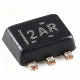
ESD9X5.0ST5G - 5V ESD TVS Diode SOD-923 | onsemi
MPN: ESD9X5.0ST5G ✓ Active| Qty | Unit Price | Extended |
|---|---|---|
| 1 | $0.04 | $0.04 |
| 10 | $0.035 | $0.35 |
| 100 | $0.028 | $2.80 |
| 500 | $0.022 | $11.00 |
| 1,000 | $0.018 | $18.00 |
ESD9X5.0ST5G Overview
A TVS (Transient Voltage Suppressors) diode is a clamping device that reacts to electrostatic discharge and other fast transient overvoltage events within nanoseconds, diverting damaging current away from sensitive ICs. Within the semiconductor hierarchy, the ESD9X5.0ST5G belongs to the ESD protection diode family, a subset of the TVS diode category, which itself sits under discrete protection semiconductors in circuit-protection systems.
Key features include excellent clamping capability, low leakage current, and fast response time, which onsemi describes as providing best-in-class protection for designs exposed to ESD threats. The device withstands ESD strikes up to +/-30kV per distributor listings and handles 8.7A of peak pulse current on the industry-standard 8/20us waveform. Its 5V reverse standoff voltage makes it suitable for protecting 5V and lower logic rails without significant loading.
The ESD9X Series architecture uses a silicon avalanche clamping structure that activates within nanoseconds of a transient event. Unlike crowbar-type protection devices, it clamps without latching, returning to a high-impedance state automatically after the surge passes. Low junction capacitance keeps signal integrity intact on moderately fast digital lines.
Typical applications include cellular phones, MP3 players, digital cameras, and other portable electronics where board space is at a premium. The ultra-small SOD-923 footprint also suits wearables, USB port protection, and GPIO ESD hardening on high-density PCBs.
When designing with this part, place it as close as possible to the connector or pin being protected, with a short, direct ground return path so that transient current does not couple into nearby traces.
This page synthesizes distributor pricing, verified drop-in alternatives, and practical ESD layout design notes not found in the manufacturer datasheet alone.
Drop-in alternatives for ESD9X5.0ST5G — same package, pin-to-pin compatible. Different-package parts requiring PCB rework are excluded.
Variants in this series
Same-series models that are drop-in compatible with ESD9X5.0ST5G (same form factor and footprint) — differing in Configuration, Package, Peak Pulse Current (Ipp), Polarity.
Quick Comparison Tool — Select alternative parts for side-by-side comparison:
ESD9B5.0ST5G
✅ Drop-In📋 Reference alternative (not in catalog)
ESD9X5.0ST5G
✅ Drop-In✓ In Stock
$0.018 / Unit
View Datasheet →ESD9X5.0ST5G
✅ Drop-In✓ In Stock
$0.018 / Unit
View Datasheet →ESD9X5.0ST5G Maximum Ratings & Electrical Characteristics
| Reverse Standoff Voltage (VRWM) | 5 V |
| Clamping Voltage | 12.3 V at 8.7 A (8/20us) |
| Peak Pulse Current (Ipp) | 8.7 A (8/20us) |
| Configuration | Uni-directional, single channel |
| ESD Withstand | +/-30 kV (per distributor listing) |
| Technology | TVS / ESD protection diode (avalanche clamp) |
| Package | SOD-923, 2-pin surface mount |
| Mounting Type | Surface Mount |
| Response Time | Fast response (nanosecond class, per onsemi description) |
| Polarity | Unidirectional |
| Packaging | Tape and Reel (T/R) |
ESD9X5.0ST5G Pin Configuration
| Pin 1 | K (Cathode) — Cathode - connect to the rail being protected (positive node) |
| Pin 2 | A (Anode) — Anode - connect to ground |
Typical Applications
ESD9X5.0ST5G is suitable for 6 applications: Smartphone and Mobile Device Port Protection, USB Port ESD Protection, Digital Camera and Imaging Electronics, Wearable and IoT Sensor Nodes, Industrial Control Panel GPIO Hardening, Audio Accessory and Headphone Jack Protection.
Smartphone and Mobile Device Port Protection
Smartphone connectors, SIM interfaces, and accessory ports are repeatedly exposed to human-body ESD during daily handling. The ESD9X5.0ST5G fits this application because its 5V reverse standoff voltage covers battery-charger and 5V USB inputs without conducting in normal operation, while its 12.3V clamp at 8.7A (8/20us) keeps surge voltage below the failure thresholds of baseband and PMIC pins rated for ESD. The +/-30kV ESD withstand exceeds typical IEC air-discharge test levels. Design-wise, the SOD-923 package occupies under 0.5 mm2 of board area, so it can be placed within 1-2 mm of the connector pin where ESD energy enters, which is the layout position that most determines protection effectiveness. Response time is nanosecond-class, so the clamp engages before the rising transient front reaches the protected IC. Multiple channels each get their own diode, keeping leakage low on battery-powered devices.
Recommended
USB Port ESD Protection
USB VBUS operates at 5V nominal, which aligns exactly with the 5V reverse standoff voltage of the ESD9X5.0ST5G, ensuring zero conduction leakage during normal operation. When a user inserts a cable or touches the connector shell, contact discharge currents up to several amperes on the 8/20us timescale enter the port; the diode clamps at 12.3V at its rated 8.7A Ipp, and its nanosecond response engages the avalanche path before the host transceiver sees destructive voltage. Placement within 2 mm of the VBUS pin minimizes trace inductance between the strike point and the clamp, keeping the effective clamped voltage close to the datasheet value; every nanohenry of series inductance adds L*di/dt overshoot during the fast rising edge. The 2-pin SOD-923 footprint allows one device per line, so D+, D-, and VBUS can each be individually protected with minimal routing disruption on crowded USB connector areas.
Recommended
Digital Camera and Imaging Electronics
Digital cameras pack image sensors, flexible PCBs, and external card slots into dense assemblies where user-touched doors, buttons, and card contacts are frequent ESD entry points. The ESD9X5.0ST5G suits this environment because its ultra-small SOD-923 body fits within the tight clearances around SD card and connector land patterns, and its low leakage preserves battery life in standby. The 5V standoff covers logic and memory card IO rails, while the 12.3V clamp at 8.7A prevents discharge events from propagating into the image sensor's sensitive analog front end, where a single ESD event can create permanent pixel defects. Because the diode responds in nanoseconds, it clamps the leading edge of the ESD pulse that soft-logic protection schemes would miss. onsemi explicitly lists digital cameras among target applications for the ESD9X series, and the tape-and-reel format supports high-volume automated pick-and-place assembly.
Recommended
Wearable and IoT Sensor Nodes
Wearables and battery-powered IoT sensor nodes face ESD exposure at charging contacts, touch electrodes, and exposed antennas while offering almost no spare board area. The ESD9X5.0ST5G addresses both constraints: its SOD-923 package measures roughly 1.0 x 0.6 mm, fitting beside 0201-class passives in the densest layout regions, and its low leakage current avoids eroding the microampere-scale sleep budgets that define battery life in these products. The 5V reverse standoff tolerates lithium-charger voltage transients on contact pins, and the 12.3V clamp at 8.7A (8/20us) absorbs human-body-model strikes at charging pogo pins that users touch daily. Nanosecond response time is important here because MCU IO structures are increasingly thin-oxide and unforgiving. For multi-contact designs, place one diode per exposed contact with a direct via to the ground plane; daisy-chaining ground returns adds inductance that degrades clamping during fast ESD edges.
Recommended
Industrial Control Panel GPIO Hardening
Industrial panels route operator-facing buttons, DIP switches, and status connectors over wiring harnesses that act as antennas for both ESD and cable-discharge events. The ESD9X5.0ST5G provides a low-cost per-channel first line of defense: its 5V standoff covers 5V and 3.3V PLC logic rails, its 8.7A Ipp (8/20us) rating absorbs coupling from field wiring, and the 12.3V clamp keeps transients below the absolute maximum ratings of modern CMOS logic such as 74LVC and 74HCS families. For environments with heavier surge exposure, this diode pairs with a secondary higher-power TVS such as an SMBJ series part in a staged protection network, with series resistance between stages to share energy. The SOD-923 footprint lets designers populate one diode at every panel connector pin rather than protecting groups of lines, improving per-channel clamp performance at negligible board cost in high-channel-count IO cards.
Recommended
Audio Accessory and Headphone Jack Protection
Headphone jacks and audio accessory connectors are among the most frequently touched surfaces on portable and consumer audio products, making them prime ESD entry points into codec line outputs and microphone bias circuits. The ESD9X5.0ST5G clamps positive transients at 12.3V at its 8.7A rating while its low leakage preserves the DC bias accuracy that electret and MEMS microphone circuits depend on. Its 5V standoff tolerates the mic-bias rail and line-level swings, and the nanosecond avalanche response catches the fast edge of a finger strike before it reaches the codec. The sub-0.5 mm2 SOD-923 footprint is essential in 3.5 mm jack land patterns where routing space is minimal, allowing placement directly at the jack tip, ring, and sleeve contacts. One uni-directional diode per contact provides consistent clamping without adding capacitance-heavy multi-channel arrays that can distort audio-band impedance.
Recommended
Recommended Products Summary
Engineering reference data for ESD9X5.0ST5G — comparison, design guidance, and compliance information.
Selection Guide
Comparison with Alternatives
| Parameter | This Product | ESD9B5.0ST5G | ESD9X5.0ST5G (MSKSEMI) | ESD9X5.0ST5G (GOODWORK) |
|---|---|---|---|---|
| Package | SOD-923 (2-pin) | SOD-923 - same | SOD-923 - same | SOD-923 - same |
| Brand | onsemi | onsemi | MSKSEMI | GOODWORK |
| Reverse Standoff Voltage | 5 V | 5 V | 5 V | 5 V |
| Configuration | Uni-directional | Uni-directional | Uni-directional | Uni-directional |
Key Differentiators
- Documented clamp point at full rated current (vs ESD9B5.0ST5G)
- Ultra-small footprint vs larger TVS packages (vs SMBJ6.0CA)
- Cost advantage of second-source equivalents (vs ESD9X5.0ST5G (MSKSEMI))
Design Notes
ESD protection effectiveness depends more on placement than on the diode itself. Place the ESD9X5.0ST5G within 1-2 mm of the connector pin being protected, with a short, direct via to the ground plane at the anode. Every nanohenry of trace inductance between the strike point and the clamp adds L*di/dt overshoot - with an 8/20us-class 8.7A pulse and a fast rising edge, even 5 nH of extra inductance meaningfully raises the voltage seen at the protected IC during the initial edge. Never route the protected signal away from the diode to a 'convenient' location.
Match the standoff voltage to the rail with margin: the 5V VRWM of the ESD9X5.0ST5G must exceed the maximum continuous voltage on the line, including tolerances and transients, or the diode will leak or partially conduct. Conversely, do not over-select - a 24V standoff diode on a 5V line leaves the protected IC exposed to a much higher clamped voltage. Also remember this is a uni-directional device: negative-going signal swings will be forward-biased clamped at approximately one diode drop, which is unacceptable for AC-coupled or bipolar signal lines.
Verify junction capacitance against signal speed before committing to layout. ESD protection diodes add shunt capacitance at the connector; on USB full-speed and slower lines this is usually negligible, but on fast differential pairs or high-impedance analog nodes it can degrade edges and increase jitter. Obtain the capacitance figure from the onsemi ESD9X series datasheet and, where needed, compare against lower-capacitance family variants within the ESD9X lineup. Keep the diode on the connector side of any series termination resistor so the resistor isolates the clamp capacitance from the driver.
For staged protection on power entries, pair the ESD9X5.0ST5G with a higher-power TVS (for example an SMBJ-class part) and a small series resistance between stages. The ESD9X diode reacts first at the connector due to its nanosecond response, while the SMBJ absorbs bulk surge energy downstream; the series element forces current sharing. Estimated: with 1 ohm series resistance and an 8.7A pulse, the downstream stage sees about 8.7V across the resistor, keeping each device within its rated pulse energy. Label this arrangement as an estimate and validate against your actual surge waveform.
Compliance Information
Compliance status was not explicitly stated in the provided verified web data. onsemi discrete ESD protection diodes are typically RoHS compliant, but this must be confirmed from the official product page or datasheet before specification.