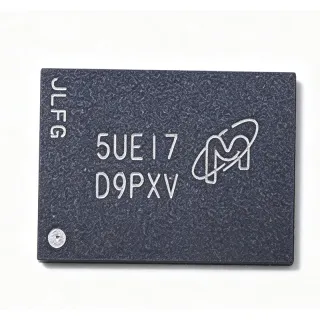
N25Q256A83ESFA0F - 256Mb SPI NOR Flash 108MHz | Micron
MPN: N25Q256A83ESFA0F ✓ Active| Qty | Unit Price | Extended |
|---|---|---|
| 1 | $3.2 | $3.20 |
| 10 | $2.88 | $28.80 |
| 100 | $2.55 | $255.00 |
| 500 | $2.3 | $1,150.00 |
| 1,000 | $2.05 | $2,050.00 |
Drop-in alternatives for N25Q256A83ESFA0F — same package, pin-to-pin compatible. Different-package parts requiring PCB rework are excluded.
Quick Comparison Tool — Select alternative parts for side-by-side comparison:
N25Q256A83ESFA0G
✅ Drop-In📋 Reference alternative (not in catalog)
N25Q256A83ESFH0F
✅ Drop-In📋 Reference alternative (not in catalog)
N25Q256A13E12A0F
✅ Drop-In ⚠️ 参数待验证✓ In Stock
Contact for price
View Datasheet →N25Q256A83ESFA0F Maximum Ratings & Electrical Characteristics
| Memory Type | NOR Flash, Serial SPI |
| Density | 256 Mbit (32 MB) |
| Organization | 32M x 8 |
| Interface | SPI, Multiple I/O (Single/Dual/Quad) |
| Max Clock Frequency | 108 MHz |
| Supply Voltage | 3 V (2.7 V to 3.6 V) |
| Technology | 65nm NOR |
| Sector Erase Size | 4 KB |
| Operating Temperature | -40C to +125C |
| Features | Execute-In-Place (XIP), Advanced Write Protection |
| Package | 16-SOIC Wide (16SO) |
| Mounting Type | Surface Mount |
| Packaging | Tape & Reel (TR) |
| RoHS Status | Compliant |
| Grade | Industrial |
N25Q256A83ESFA0F Pin Configuration
| Pin 1 | SIO3/HOLD# — Serial data I/O 3 in quad mode / Hold input |
| Pin 2 | VCC — Power supply (2.7V to 3.6V) |
| Pin 3 | NC — Not connected (per datasheet) |
| Pin 4 | NC — Not connected (per datasheet) |
| Pin 5 | NC — Not connected (per datasheet) |
| Pin 6 | NC — Not connected (per datasheet) |
| Pin 7 | SCK — Serial clock input |
| Pin 8 | SIO0 — Serial data I/O 0 (command/address/data) |
| Pin 9 | S# — Chip select (active low) |
| Pin 10 | SIO1 — Serial data I/O 1 (data output) |
| Pin 11 | SIO2 — Serial data I/O 2 in quad mode |
| Pin 12 | GND — Ground |
| Pin 13 | RESET#/SIO3 — Hardware reset / quad I/O function |
| Pin 14 | NC — Not connected (per datasheet) |
| Pin 15 | NC — Not connected (per datasheet) |
| Pin 16 | NC — Not connected (per datasheet) |
Safe Operating Area (SOA) & Thermal Characteristics
No official SOA curve available for this digital IC. Always operate within absolute maximum ratings specified in the datasheet. Ensure adequate cooling and derate as needed.
Typical Applications
N25Q256A83ESFA0F is suitable for 6 applications: Embedded Boot Code Storage, Industrial Automation Controllers, Networking and Telecom Equipment, FPGA Configuration Storage, Set-Top Box and Display Modules, Automotive-Adjacent Telematics.
Embedded Boot Code Storage
The N25Q256A83ESFA0F is a primary choice for boot-code storage in embedded processors, MCUs, and FPGAs. Its 108 MHz multiple-I/O SPI interface in quad mode delivers the read bandwidth needed for fast boot times, while execute-in-place (XIP) support lets the host run initialization code directly from flash without a RAM copy step. The 4 KB sector erase granularity allows fine-grained updates of bootloader parameters without erasing the whole array. Placed on the SPI bus of the host SoC with 0.1uF decoupling on VCC, the 32 MB capacity comfortably holds bootloader, firmware image, and fallback recovery images for industrial controllers.
Recommended
Industrial Automation Controllers
Industrial PLCs, motor drives, and factory automation controllers benefit directly from the N25Q256A83ESFA0F's -40C to +125C operating range, which covers cold warehouses and hot panel enclosures without derating. The 3V supply integrates cleanly with standard 3.3V logic rails, and the advanced write-protection mechanism guards critical firmware regions against accidental or malicious modification during long service life. Its 256 Mbit capacity stores application logic, configuration data, and event logs, while quad SPI reads keep firmware checksum verification fast during power-on self-test cycles in high-availability production lines.
Recommended
Networking and Telecom Equipment
Routers, switches, and base-station line cards use the N25Q256A83ESFA0F to store firmware images, device trees, and factory calibration data. Quad SPI at 108 MHz provides the throughput for rapid image authentication and dual-bank firmware schemes, where the 32 MB array holds a primary and a backup image with room to spare. XIP operation supports processors that execute early boot code directly from NOR before loading the main OS from NAND or eMMC. The wide SOIC package reflows reliably on standard telecom assembly lines and withstands the extended temperature profiles of outdoor telecom cabinets.
Recommended
FPGA Configuration Storage
FPGA platforms commonly load their bitstreams from serial NOR flash at power-up, and the N25Q256A83ESFA0F fits this role for mid-to-large FPGAs whose compressed bitstreams approach tens of megabits. The 108 MHz quad SPI read satisfies typical FPGA configuration-time requirements, and 32 MB leaves headroom for multiple configuration images plus a golden image for remote-update recovery. The advanced sector protection lets designers lock the golden image permanently while leaving user-update regions rewritable, an important field-reliability feature for deployed industrial and communications hardware.
Recommended
Set-Top Box and Display Modules
Set-top boxes, smart displays, and HMI panels store boot firmware, graphical assets, and user settings in the N25Q256A83ESFA0F. The multiple-I/O SPI bus keeps the PCB interconnect minimal (six signals plus power) compared with parallel NOR, saving board layers in cost-sensitive consumer platforms. Execute-in-place support allows the display controller to fetch glyph and asset tables directly from flash, reducing RAM requirements. Its wide operating range also accommodates enclosed consumer products with limited ventilation where internal temperatures exceed standard commercial limits.
Recommended
Automotive-Adjacent Telematics
Telematics units, fleet trackers, and dashboard display controllers in the extended-temperature supply chain use the N25Q256A83ESFA0F where -40C to +125C tolerance and robust write protection are required, even for non-AEC-Q100-qualified positions. Quad SPI XIP allows the modem processor to boot quickly from flash, and the 256 Mbit array stores map caches, log data, and dual firmware banks for over-the-air updates with rollback protection. Designers should confirm the exact qualification requirement of their position; for formal automotive qualification, consult Micron's automotive-grade variants.
Recommended
Recommended Products Summary
Engineering reference data for N25Q256A83ESFA0F — comparison, design guidance, and compliance information.
Selection Guide
Comparison with Alternatives
| Parameter | This Product | N25Q256A83ESFA0G | N25Q256A83ESFH0F | N25Q256A13E12A0F |
|---|---|---|---|---|
| Package | 16-SOIC Wide (16SO) | 16-SOIC Wide - same | 16-SOIC Wide - same | N25Q family 256Mb - verify footprint |
| Brand | Micron Technology | Micron Technology | Micron Technology | Micron Technology |
| Density | 256 Mbit (32 MB) | 256 Mbit | 256 Mbit | 256 Mbit |
| Max Clock Frequency | 108 MHz | 108 MHz | 108 MHz | 108 MHz |
| Supply Voltage | 3 V (2.7V-3.6V) | 3 V | 3 V | 3 V |
| Operating Temperature | -40C to +125C | -40C to +125C | Extended grade per 'H' coding | Per '13E12' coding - verify |
| Sector Erase Size | 4 KB | 4 KB | 4 KB | 4 KB |
| XIP Support | Yes | Yes | Yes | Yes |
Key Differentiators
- Industrial -40C to +125C range in standard package (vs N25Q256A13E12A0F)
- Newer stepping availability without redesign (vs N25Q256A83ESFA0G)
- Extended temperature upgrade path on same PCB (vs N25Q256A83ESFH0F)
Design Notes
Decouple VCC (pin 2) with a 0.1uF ceramic capacitor placed within 2 mm of the pin, plus a 10uF bulk capacitor per device on the 3.3V rail. Programming and erase operations cause current transients on the supply; an under-decoupled rail can produce brownout-induced write corruption that appears as random bit failures in the field. Route VCC and GND as a small plane pair under the SOIC-16 footprint rather than long thin traces.
At 108 MHz quad SPI, treat the four SIO lines and SCK as moderately fast signals: keep trace lengths matched within a few centimeters, avoid stubs, and insert 22-33 ohm series resistors near the flash if the host is more than 10 cm away. Above 54 MHz, verify that the host SPI controller supports the required timing (clock-to-output and setup/hold margins) per the Micron datasheet AC tables; do not assume dual-mode timing margins carry to quad mode.
The 256Mb array exceeds the 24-bit (16 MB) addressing space, so 4-byte addressing or the extended address register must be used for upper addresses; firmware that assumes 24-bit-only addressing will wrap and corrupt data in the upper 16 MB. Also terminate HOLD#/RESET#/SIO3 appropriately for your mode - floating hold/reset pins are a frequent cause of intermittent boot failures. Verify erase-before-write discipline: the device can only program bits from 1 to 0.
Compliance Information
RoHS compliant per distributor listings (DigiKey, Mouser). Formal REACH, halogen-free, and conflict-minerals declarations should be obtained from Micron's official product environmental documentation.