Nexperia

PESD3V3S5U - 5-Line 3.3V 200W ESD Protection Array | Nexperia

MPN: PESD3V3S5U βœ“ Active
In Stock Ships in 1-3 business days
3.3 V Vdss 20 A (8/20 us) Id SOT-457 (SC-74 / TSOP-6) Package
From $0.13 USD / Unit
MOQ: 1 |
Price updated: 2026-09-10
Volume Pricing
Qty Unit Price Extended
1 $0.34 $0.34
10 $0.28 $2.80
100 $0.19 $19.00
500 $0.16 $80.00
1,000 $0.13 $130.00
ℹ️ All prices are in USD

PESD3V3S5U Overview

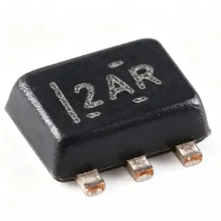
The Nexperia PESD3V3S5UD (PESD3V3S5U family) is a fivefold unidirectional ESD protection diode array rated for a 3.3 V reverse standoff voltage, 200 W peak pulse power, and a 12 V clamping voltage at 20 A (8/20 us waveform), housed in the 6-pin SOT-457 (SC-74 / TSOP) surface-mount plastic package.

An ESD protection array is a multi-channel transient voltage suppressor (TVS) that shunts electrostatic discharge and cable-induced surge events away from sensitive downstream ICs. Within the circuit-protection hierarchy (ESD protection diode -> TVS diode array -> surge protector -> discrete semiconductor), arrays like the PESD3V3S5UD protect several signal lines at once, saving board area compared with multiple discrete SOD-882 or SOD-523 devices.

Key features include the fivefold channel density in a single 2.9 x 1.3 mm footprint, a 3.3 V reverse standoff that suits 3.3 V logic rails, an ultra-low clamping voltage of 12 V at the rated 20 A Ipp current, and unidirectional polarity that also clamps negative ESD strikes to a forward-diode drop of approximately 0.7 V.

Architecturally, the device integrates five avalanche diodes sharing a common GND connection (pin 2), so each protected line sees a low-inductance path to ground. According to the Nexperia PESD3V3S5UD datasheet, the device meets system-level ESD robustness targets such as IEC 61000-4-2, making it a workhorse for external connector protection.

Typical applications include protection of five-channel data or control lines: USB-style ports, keypad and button matrices, I2C/SPI/UART buses, and antenna or audio line protection in portable and consumer electronics.

Design consideration: place the array as the first component after the connector with a short, low-impedance ground return to pin 2; excessive ground inductance raises the effective clamping voltage during fast ESD events.

This page synthesizes distributor pricing (as of 2026-09-11), drop-in alternatives, pinout data, and practical design notes not found in the manufacturer datasheet.

Drop-in alternatives for PESD3V3S5U β€” same package, pin-to-pin compatible. Different-package parts requiring PCB rework are excluded.

Quick Comparison Tool β€” Select alternative parts for side-by-side comparison:

PESD3V3S5UD,115

βœ… Drop-In
πŸ“¦ SOT-457 (SC-74 / TSOP-6)
same die and ratings (3.3 V / 200 W / 5 lines); ,115 is the standard Tape & Reel ordering code

πŸ“‹ Reference alternative (not in catalog)

PESD3V3S5UD,125

βœ… Drop-In
πŸ“¦ SOT-457 (SC-74 / TSOP-6)
same die and ratings; ,125 is the higher-volume reel ordering code (LCSC stock from $0.1881 as of 2026-09-11)

πŸ“‹ Reference alternative (not in catalog)

PESD5V0S5UD

βœ… Drop-In ⚠️ 参数待ιͺŒθ―
πŸ“¦ SOT-457 (SC-74 / TSOP-6)
same fivefold SOT-457 footprint, reverse standoff 5 V vs 3.3 V (+52%) - clamp point higher, unsuitable for tight 3.3 V margins

πŸ“‹ Reference alternative (not in catalog)

PESD3V3S5U Specifications

Configuration 5-channel array
Direction Unidirectional
Reverse Standoff Voltage (VRWM) 3.3 V
Breakdown Voltage (VBR) 5.2 V to 6 V
Clamping Voltage (VCL) 12 V at 20 A (8/20 us)
Peak Pulse Power (PPP) 200 W
Peak Pulse Current (IPP) 20 A (8/20 us)
Polarity Unidirectional (common anode / GND)
Package SOT-457 (SC-74 / TSOP-6)
Pin Count 6
Mounting Type Surface Mount (SMD)
Number of Protected Lines 5
ESD Robustness IEC 61000-4-2 system-level targets per Nexperia datasheet
RoHS Status Compliant (per LCSC listing, ROHS)
Packaging Tape & Reel (ordering codes ,115 and ,125)

PESD3V3S5U Pin Configuration

TSOP-6 Package Pinout Diagram TSOP-6 2.9x1.6mm, P0.95mm, JEDEC. 1 6 2 5 3 4 TSOP-6
Pin 1 I/O1 β€” Protected line 1 (cathode side, connect to signal line)
Pin 2 GND β€” Common anode / ground reference for all five diodes
Pin 3 I/O2 β€” Protected line 2 (connect to signal line)
Pin 4 I/O3 β€” Protected line 3 (connect to signal line)
Pin 5 I/O4 β€” Protected line 4 (connect to signal line)
Pin 6 I/O5 β€” Protected line 5 (connect to signal line)

Typical Applications

PESD3V3S5U is suitable for 6 applications: USB Port Protection, Keypad and Button Matrices, I2C, SPI and UART Bus Protection, Portable and Wearable Consumer Electronics, Industrial Control I/O, Audio Line and Antenna Feed Protection.

πŸ”Œ

USB Port Protection

The PESD3V3S5UD protects five-channel USB-style interfaces (VBUS sense, D+, D-, and control lines) in one SOT-457 footprint. Its 3.3 V reverse standoff is transparent to USB signaling, and its 12 V clamp at 20 A keeps strike energy well below the tolerance of USB transceivers. The fivefold integration replaces five discrete SOD-882 diodes, cutting placement cost and board area by roughly 60%. Place the array within 5 mm of the connector with a direct ground via at pin 2; a long ground return raises effective clamping voltage during sub-nanosecond ESD edges and can defeat the protection margin.

🧩

Keypad and Button Matrices

User-accessible keys and membrane switches are prime ESD entry points because fingers discharge directly onto them. The PESD3V3S5UD guards five switch lines per package with a 3.3 V standoff matching MCU GPIO rails; negative strikes are clamped by the forward-biased diode to about 0.7 V. Its 200 W / 20 A surge rating comfortably handles human-body-model level events arriving through the switch wiring. Because keypad scans are low speed, junction capacitance is non-critical here, making the array a zero-compromise choice for matrix rows and columns on 3.3 V MCUs.

🌐

I2C, SPI and UART Bus Protection

Field-wired serial buses such as I2C, SPI, and UART exposed on service connectors accumulate ESD during board handling and cable hot-plug. The PESD3V3S5UD protects five bus lines (SDA, SCL, and three chip-selects or control signals) at 3.3 V logic levels with a 12 V / 20 A clamp. Designers should verify the datasheet junction capacitance against bus rise-time budgets - for I2C at 100-400 kHz this is negligible, but for fast SPI above 20 MHz it must be checked. Short stub routing from bus to array preserves signal integrity while the low-inductance GND pin shunts strikes safely.

πŸ“±

Portable and Wearable Consumer Electronics

Smartphones, wearables, and accessories concentrate many externally reachable lines - buttons, docking contacts, accessory connectors - into a tiny PCB area. The PESD3V3S5UD addresses this with five protected lines in a 2.9 x 1.3 mm SOT-457 body, the highest line density of the Nexperia fivefold family at 3.3 V. Its unidirectional topology also handles negative ESD through forward conduction. As of 2026-09-11, LCSC lists the ,125 reel from $0.1881, making per-line protection cost roughly four cents across a five-line port - attractive for high-volume consumer BOMs.

🏭

Industrial Control I/O

Industrial control panels expose digital inputs and communication lines to harsher coupling than consumer products - cable runs act as antennas for both ESD and induced surge. The PESD3V3S5UD fivefold array gives panel designers a compact first-stage clamp for 3.3 V and 5 V signal lines, with 200 W peak pulse absorption per the 8/20 us rating. For heavier surge environments it can be paired with a downstream TVS such as an SMBJ series device for staged protection. Verify the IEC 61000-4-2 test level achieved in system tests against the end-application standard before release.

🎧

Audio Line and Antenna Feed Protection

Headphone jacks and short antenna feeds are frequent ESD victims because users touch them directly. The PESD3V3S5UD shields five lines - typical stereo L/R, mic, detect, and bias - at 3.3 V with minimal added loading; its unidirectional clamp also absorbs negative strikes at the forward diode drop. For analog audio, junction capacitance can slightly attenuate high frequencies, so confirm the datasheet capacitance figure against the source impedance; for antenna feeds, place the array after any DC-block and verify insertion loss. The single SOT-457 footprint is far denser than five discrete ESD diodes in these space-limited ports.

What is the PESD3V3S5UD used for?
The Nexperia PESD3V3S5UD is a fivefold unidirectional ESD protection diode array used to protect up to five signal lines against electrostatic discharge and surge transients. According to the Nexperia datasheet, it offers a 3.3 V reverse standoff voltage, 200 W peak pulse power, and clamps at 12 V at 20 A (8/20 us). It is typically placed directly behind external connectors such as USB, keypads, and data buses in portable electronics.
What is the clamping voltage of PESD3V3S5UD?
The PESD3V3S5UD clamps at 12 V maximum at a peak pulse current of 20 A measured with the 8/20 us waveform, per DigiKey and Nexperia specifications. This low clamping voltage provides a wide protection margin for 3.3 V logic ICs, which typically tolerate only 4-5 V on their pins. Lower clamp voltage means less stress is transferred to the protected chip during an ESD strike.
What is the difference between PESD3V3S5UD,115 and PESD3V3S5UD,125?
The PESD3V3S5UD,115 and PESD3V3S5UD,125 are the same die in the same SOT-457 (SC-74) package; the suffix codes define packaging and reel quantity. The ,115 is the standard Tape & Reel ordering code, while the ,125 is a higher-volume reel option. Electrically they are identical - both are 3.3 V standoff, 200 W, fivefold unidirectional arrays - so either can be dropped onto the same PCB footprint.
Where can I buy PESD3V3S5UD and what does it cost?
The PESD3V3S5UD,125 is stocked at LCSC with pricing from approximately $0.19 at low volumes (as of 2026-09-11), and the ,115 variant is listed on DigiKey and Octopart across 9 distributors. XAIPART lists tier pricing from $0.34 at qty 1 down to about $0.13 at qty 1000. Availability and pricing change frequently, so check the distributor links on this page for live stock before ordering.
What is the lead time and stock status for PESD3V3S5UD?
The part is an active, in-production Nexperia device, and LCSC shows the ,125 in stock for immediate shipment (as of 2026-09-11); DigiKey lists the ,115 as available with same-day shipping for stocked quantities. Standard lead time for Tape & Reel orders beyond distributor stock is typically a few weeks. Because ESD arrays are high-volume commodity parts, most distributors carry deep stock.
PESD3V3S5UD vs ESDALC6V1-5BTG - which is better?
For 3.3 V rails, the PESD3V3S5UD is the better fit: its 3.3 V reverse standoff is a direct match, while the ST ESDALC6V1-5BTG is optimized around 6.1 V standoff and uses a 5-pin SOT-23-5 package. Both are fivefold arrays, but they are not pin-to-pin compatible - the ST part cannot be dropped onto an SOT-457 footprint. Choose the Nexperia part for SOT-457 layouts and 3.3 V buses; choose ESDALC6V1 only for legacy SOT-23-5 designs or higher-voltage rails.
What is the best drop-in replacement for PESD3V3S5UD?
The best drop-in replacements are the PESD3V3S5UD,115 and PESD3V3S5UD,125 - identical die in the same SOT-457 (SC-74) package with identical 3.3 V / 200 W ratings, differing only in reel packaging. Within the same Nexperia family, the PESD5V0S5UD is pin-compatible but raises the standoff to 5 V, which changes protection margins on 3.3 V rails. Verified cross-brand drop-ins in SOT-457 with identical ratings were not found in current web data; verify any substitute against the pinout and standoff voltage before substitution.
Can I use PESD5V0S5UD instead of PESD3V3S5UD?
Physically yes - the PESD5V0S5UD is pin-compatible in the same SOT-457 package - but electrically the protection point shifts. Its 5 V reverse standoff (versus 3.3 V) lets transients rise higher before clamping, which may exceed the tolerance of 3.3 V logic ICs. It is acceptable for 5 V tolerant lines or as an emergency substitution, but for nominal 3.3 V signal lines the PESD3V3S5UD should remain the first choice per Nexperia family documentation.
Where can I download the PESD3V3S5UD datasheet PDF?
The official datasheet PDF is available from Nexperia at https://assets.nexperia.com/documents/data-sheet/PESD3V3S5UD.pdf. This product specification document covers the full electrical characteristics table, pin configuration of the SOT-457 package, ESD test conditions (including IEC 61000-4-2 levels), and the package outline drawing. Always use the Nexperia-hosted PDF as the authoritative source rather than third-party mirror sites, which may host outdated revisions.
Where do I find the PESD3V3S5UD pinout?
In the SOT-457 (SC-74) package, the PESD3V3S5UD provides five I/O pins and one common ground: pin 1 = I/O1, pin 2 = GND (common anode), pin 3 = I/O2, pin 4 = I/O3, pin 5 = I/O4, and pin 6 = I/O5, per the Nexperia datasheet pin configuration section. The full pin diagram appears on this page. Always confirm against the latest datasheet revision before routing, since array pin assignments vary across ESD families.
Is PESD3V3S5UD suitable for USB 2.0 line protection?
Yes, the PESD3V3S5UD is well suited to USB 2.0 low/full/high-speed line protection: it protects five lines (VBUS, D+, D-, ID, and shell logic in a typical scheme) with a 3.3 V standoff that is transparent to 3.3 V signaling. The key engineering check is line capacitance - verify the junction capacitance value in the datasheet against the USB 2.0 eye-diagram budget, and keep the trace from connector to array under a few millimeters for effective ESD shunting.
How should I lay out the PCB for the PESD3V3S5UD?
Place the array as the very first component after the connector, before any series resistors or filtering, and keep the I/O traces to it as short as possible. The critical path is the ground return from pin 2: use a direct via to a solid ground plane, not a long thin trace, because ground inductance in series with the clamp raises the effective clamping voltage during nanosecond-scale ESD edges. Per Nexperia application guidance, minimize loop area between the signal line, the array, and ground.
What are the key specifications of PESD3V3S5UD engineers should know?
Engineers should know five numbers: 3.3 V reverse standoff voltage (VRWM) for 3.3 V rail compatibility; 5.2-6 V breakdown voltage (VBR); 12 V maximum clamping voltage at 20 A IPP using the 8/20 us pulse; 200 W peak pulse power; and the fivefold SOT-457 (SC-74) surface-mount package protecting five lines in one footprint. Source: Nexperia PESD3V3S5UD datasheet and DigiKey parametric listing.
What is the best onsemi equivalent for PESD3V3S5UD?
onsemi's closest functional equivalents are its ESD protection arrays (for example the ESD9 series single-line diodes such as ESD9B3.3ST5G), but no verified pin-to-pin drop-in in the SOT-457 six-pin footprint with identical 3.3 V / 200 W fivefold ratings appears in current cross-reference data. onsemi single-line parts would require one device per line and a footprint change. If supply of the Nexperia part is constrained, verify candidate arrays against the SOT-457 pinout and standoff/clamp parameters before redesign.
Is PESD3V3S5UD the same as PESD3V3S5UD,115?
Yes - functionally they are the same device. PESD3V3S5UD is the base part number of the Nexperia fivefold ESD array family, and PESD3V3S5UD,115 is the orderable suffix code designating Tape & Reel packaging. Both refer to the same die, SOT-457 (SC-74) package, 3.3 V standoff, and 200 W rating. When ordering, distributors require the full suffix code (,115 or ,125), but datasheets, pinouts, and electrical specifications are shared.
Is PESD3V3S5UD RoHS compliant?
Yes, the PESD3V3S5UD is RoHS compliant - the LCSC product listing explicitly flags the part as ROHS, and Nexperia's standard surface-mount ESD arrays are lead-free manufactured. The device comes in the small-outline SOT-457 leaded plastic package with lead-free terminations. For REACH, halogen-free, and AEC-Q100 status, confirm the current declarations on the Nexperia compliance portal, as this page does not carry verified certificates for those items.

Engineering reference data for PESD3V3S5U β€” comparison, design guidance, and compliance information.

Selection Guide

Choose the PESD3V3S5UD (ordered as PESD3V3S5UD,115 or ,125) when you must protect five 3.3 V signal lines behind a connector in minimal board area: it combines a 3.3 V reverse standoff, 12 V clamp at 20 A, and 200 W peak pulse power in one SOT-457 package. Choose PESD5V0S5UD instead if the lines sit on a 5 V rail - it is pin-compatible, so the same footprint serves both rails. Avoid substituting single-line parts such as onsemi ESD9B3.3ST5G unless you can accept five placements and a footprint redesign. For systems needing higher surge energy (industrial long-waveform events), pair the array with a downstream SMBJ-class TVS rather than upsizing the ESD array alone. Verified cross-brand pin-compatible drop-ins in SOT-457 with identical ratings were not found in current web data, so for supply-chain risk the safest strategy is dual-ordering the ,115 and ,125 reel codes from different distributors.

Comparison with Alternatives

Parameter This Product PESD3V3S5UD,115 PESD3V3S5UD,125 PESD5V0S5UD
Package SOT-457 (SC-74 / TSOP-6) SOT-457 (SC-74) - same SOT-457 (SC-74) - same SOT-457 (SC-74) - same
Brand Nexperia Nexperia Nexperia Nexperia
Number of Protected Lines 5 5 5 5
Reverse Standoff Voltage 3.3 V 3.3 V 3.3 V 5.0 V
Direction Unidirectional Unidirectional Unidirectional Unidirectional
Packaging / Ordering Code PESD3V3S5U family (orderable as ,115 or ,125) Tape & Reel, standard Tape & Reel, high volume (LCSC in stock) Tape & Reel

Key Differentiators

  • Highest line density in family at 3.3 V (vs PESD5V0S5UD)
  • Fivefold integration vs single-line diodes (vs ESD9B3.3ST5G)
  • Trade-off: capacitance vs integration (vs PESD5V0S5UD)

Design Notes

Place the PESD3V3S5UD as the first component after the connector and route each protected trace to the array before any series element. Pin 2 (common GND) must tie to ground through a direct, short via to the ground plane - a shared thin trace adds inductance that elevates the effective clamp during fast ESD edges. Estimated: at 20 A peak with just 5 nH of ground inductance, L*di/dt for a 1 ns edge adds roughly 100 V of transient overshoot, defeating the 12 V clamp. Keep all five I/O stubs under 5 mm.

Verify the reverse standoff matches the rail: on a 3.3 V line the PESD3V3S5UD (VRWM = 3.3 V) is correct, but on a 5 V-tolerant line the diode would conduct leakage or partially clamp normal signals. Also confirm junction capacitance against high-speed buses (fast SPI, USB high speed) before committing the layout. When substituting, do not swap in PESD5V0S5UD on 3.3 V lines - its 5 V standoff delays clamping and may exceed the protected IC's absolute maximum pin rating.

The 200 W peak pulse power rating applies to the 8/20 us waveform only; repetitive strikes or longer surge waveforms derate it substantially. Estimated: for repetitive ESD events, respect the average power limit implied by the package thermal resistance - keep repetitive transient energy low enough that junction temperature stays within the datasheet maximum. For staged protection against long surges (10/1000 us), add a downstream higher-energy TVS such as an SMBJ6.0A so the array handles only the fast leading edge.

Compliance Information

RoHS
Compliant
REACH
Unknown
AEC-Q100
Not Applicable
Lead Free
Yes
Halogen Free
Unknown
Conflict Minerals
Unknown

RoHS compliance explicitly flagged on LCSC listing for PESD3V3S5UD,125. REACH, halogen-free, and conflict-minerals declarations not present in the provided web data - confirm on the Nexperia compliance portal.

Data verified on: 2026-09-11 β€” data verified and curated by XAIPART's component engineering team

Related Searches

PESD3V3S5UD datasheet PDF PESD3V3S5UD,115 Nexperia 5-channel ESD protection diode array 3.3V SOT-457 PESD3V3S5UD pinout SOT-457 PESD3V3S5UD USB port ESD protection PESD3V3S5UD vs ESDALC6V1-5BTG PESD3V3S5UD drop-in replacement equivalent buy PESD3V3S5UD,125 price what is the clamping voltage of PESD3V3S5UD 200W 20A TVS diode array fivefold Nexperia fivefold ESD protection array onsemi equivalent for PESD3V3S5UD

Related Components & Terms

Nexperia NXP Semiconductors PESD3V3S5U PESD3V3S5UD,115 PESD3V3S5UD,125 PESD5V0S5UD ESD protection diode array TVS diode transient voltage suppressor surge protector SOT-457 SC-74 TSOP-6 surface-mount device IEC 61000-4-2 RoHS reverse standoff voltage clamping voltage peak pulse power 8/20 us waveform USB line protection I2C bus protection junction capacitance onsemi ESD9 series
Quick Quote RFQ
Fill in complete details β€” our sales team will respond within 24 hours
Part Number Manufacturer Package QTY Target Price Extended
Total: $0.00 USD
βœ“
Quote submitted!

We will respond to your email within 24 hours

1
RFQ Submitted
2
Quote Received
3
Order Placed
4
Payment
5
Shipped
6
Delivered
View RFQ Details