Texas Instruments

SN74AVC4T245PWR - 4-Bit Dual-Supply Level Shifter | TI

MPN: SN74AVC4T245PWR βœ“ Active
In Stock Ships in 1-3 business days
0.8 V to 3.6 V Vdss 16-TSSOP (PW), 4.4 mm body width, 0.65 mm pin pitch Package
From $0.38 USD / Unit
MOQ: 1 |
Price updated: 2026-09-03
Volume Pricing
Qty Unit Price Extended
1 $0.72 $0.72
10 $0.63 $6.30
100 $0.51 $51.00
500 $0.44 $220.00
1,000 $0.38 $380.00
ℹ️ All prices are in USD

Drop-in alternatives for SN74AVC4T245PWR β€” same package, pin-to-pin compatible. Different-package parts requiring PCB rework are excluded.

Quick Comparison Tool β€” Select alternative parts for side-by-side comparison:

SN74AVC4T245QPWRQ1

βœ… Drop-In
πŸ“¦ 16-TSSOP (PW)
same die function and pinout, AEC-Q100 automotive qualified, extended temp range

πŸ“‹ Reference alternative (not in catalog)

SN74AVCH4T245PWR

βœ… Drop-In
πŸ“¦ 16-TSSOP (PW)
same 4-bit AVC transceiver, AVCH grade with extended dynamic-drive specification conditions

πŸ“‹ Reference alternative (not in catalog)

SN74AXC4T245PWR

βœ… Drop-In
πŸ“¦ 16-TSSOP (PW)
newer AXC generation, updated dynamic-drive specs, VCC range shift (1.0V-class floor vs 0.8V floor)

πŸ“‹ Reference alternative (not in catalog)

SN74LVC4T245PWR

βœ… Drop-In ⚠️ 参数待ιͺŒθ―
πŸ“¦ 16-TSSOP (PW)
LVC family: max data rate ~100 Mbps vs 380 Mbps (-74%), lower cost otherwise pin-to-pin

πŸ“‹ Reference alternative (not in catalog)

SN74AVC4T245PWR Maximum Ratings & Electrical Characteristics

Function 4-bit dual-supply bus transceiver with configurable voltage translation
VCCA Supply Range 0.8 V to 3.6 V
VCCB Supply Range 0.8 V to 3.6 V
Translation Type Bidirectional, configurable (down/up translation both ports)
Bits per Element 2 elements, 2 bits per element (4-bit total)
Output Type 3-State
Max Data Rate 380 Mbps
Typical Propagation Delay 2.5 ns
Control Input Reference VCCA (1DIR, 2DIR, 1OE, 2OE)
Ioff Partial-Power-Down Yes
VCC Isolation Feature Yes (all I/O high impedance if either rail at GND)
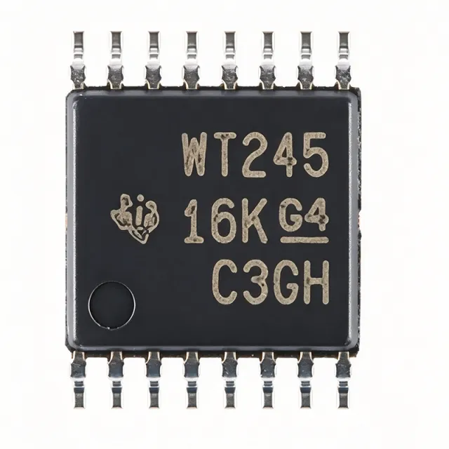
Package 16-TSSOP (PW), 4.4 mm body width, 0.65 mm pin pitch
Operating Temperature -40C to +85C
Mounting Type Surface Mount
Marking Code WT245
AEC-Q100 Qualification Not applicable (choose SN74AVC4T245QPWRQ1 for AEC-Q100 automotive grade)

SN74AVC4T245PWR Pin Configuration

TSSOP-16 Package Pinout Diagram TSSOP-16 4.4x5mm, P0.65mm, JEDEC MO-153. 1 16 2 15 3 14 4 13 5 12 6 11 7 10 8 9 TSSOP-16
Pin 1 1DIR β€” Direction control for port 1 (VCCA-referenced)
Pin 2 1OE β€” Output enable for port 1 (VCCA-referenced)
Pin 3 VCCA β€” A-port supply, 0.8V to 3.6V
Pin 4 A1 β€” A-port data I/O, bit 1
Pin 5 A2 β€” A-port data I/O, bit 2
Pin 6 GND β€” Ground
Pin 7 A3 β€” A-port data I/O, bit 3
Pin 8 A4 β€” A-port data I/O, bit 4
Pin 9 2DIR β€” Direction control for port 2 (VCCA-referenced)
Pin 10 2OE β€” Output enable for port 2 (VCCA-referenced)
Pin 11 B4 β€” B-port data I/O, bit 4
Pin 12 B3 β€” B-port data I/O, bit 3
Pin 13 VCCB β€” B-port supply, 0.8V to 3.6V
Pin 14 B2 β€” B-port data I/O, bit 2
Pin 15 B1 β€” B-port data I/O, bit 1
Pin 16 GND β€” Ground

Safe Operating Area (SOA) & Thermal Characteristics

Safe Operating Area Chart Default safe operating area chart for SN74AVC4T245PWR Drain-to-Source Voltage (Vds) Drain Current (Id)

No official SOA curve available for this digital IC. Always operate within absolute maximum ratings specified in the datasheet. Ensure adequate cooling and derate as needed.

Typical Applications

SN74AVC4T245PWR is suitable for 6 applications: SPI Bus Level Shifting, FPGA and ASIC Bank Interconnect, Industrial Control Systems, Portable Battery-Powered Electronics, Automotive Modules (Q1 Variant), UART and GPIO Expansion.

πŸ”§

SPI Bus Level Shifting

The SN74AVC4T245PWR is an excellent SPI level shifter because its 380 Mbps data rate and 2.5 ns typical propagation delay comfortably support SPI clocks up to tens of MHz with minimal timing skew. One channel pair handles MOSI/SCLK from controller to peripheral while the other pair returns MISO, with DIR pins set per direction and 1OE/2OE gating each element independently. Placed between a 1.8V MCU and a 3.3V sensor bank, the device adds negligible delay to SPI timing budgets. Because control inputs are referenced to VCCA, the 1.8V controller drives direction and enable directly without extra translation. Add 0.1uF decoupling on both rails and keep traces short to preserve edge integrity at high SCLK rates.

πŸ–₯️

FPGA and ASIC Bank Interconnect

Modern FPGAs and ASICs frequently mix 1.8V I/O banks with 3.3V legacy peripherals; the SN74AVC4T245PWR bridges these domains bidirectionally with its 0.8V to 3.6V dual-rail range. Its 2.5 ns propagation delay keeps setup-and-hold margins intact for parallel address/data buses, and 3-state outputs allow the transceiver to release the bus during high-impedance phases for shared-bus topologies. The VCC isolation feature protects the FPGA during power sequencing by forcing all I/O high-impedance if either rail is absent, avoiding latch-up stress on bank pins. With four bits per package, two devices serve an 8-bit parallel interface, and the 16-TSSOP footprint conserves board area near dense FPGA escape routing.

🏭

Industrial Control Systems

Industrial controllers routinely mix 3.3V microcontrollers with 5V-tolerant-tolerated or 2.5V PLC-adjacent logic; the SN74AVC4T245PWR provides robust translation in its -40C to +85C industrial temperature range. The Ioff partial-power-down circuitry prevents damaging backflow current when subsystems power down independently, a common condition in modular industrial cabinets where boards are hot-plugged or selectively de-energized. Direction control referenced to VCCA simplifies interfacing with the 3.3V main MCU. The 380 Mbps capability also covers fast incremental-encoder and parallel communication interfaces. Designers should sequence DIR changes through a brief high-impedance interval via the OE pins to prevent bus contention when reversing a shared industrial data bus.

πŸ“±

Portable Battery-Powered Electronics

Battery-powered products often combine a low-voltage (1.2V or 1.8V) application processor with 3.3V peripheral ICs, and the SN74AVC4T245PWR's 0.8V minimum rail support accommodates deep sub-1V-class core-adjacent I/O as batteries discharge. The Ioff circuitry is particularly valuable in portable designs: when a subsystem is switched off for power saving, the transceiver outputs go high-impedance and block backflow current that would otherwise drain the battery or damage powered-down ICs. The small 16-TSSOP package with 0.65mm pitch suits dense handheld PCBs. At a typical $0.38-$0.72 unit price (as of 2026-09-03), the BOM impact is minimal for consumer electronics platforms.

πŸš—

Automotive Modules (Q1 Variant)

Automotive ECUs and body-control modules require AEC-Q100 qualification, so designers should specify the SN74AVC4T245QPWRQ1, which is the identical die function and TSSOP-16 pinout qualified for automotive use. Translation tasks mirror the standard part: bridging 1.8V/3.3V domains between microcontrollers, CAN/LIN transceiver digital sides, and sensor arrays. The VCC isolation and Ioff features address automotive power-moding, where individual rails collapse during crank or partial-sleep states without damaging I/O. Because the Q1 part is pin-to-pin identical, dual-sourcing the standard SN74AVC4T245PWR for non-automotive SKUs shares one PCB footprint across product families, reducing qualification and inventory overhead for tier-one suppliers.

🧩

UART and GPIO Expansion

UART links, status lines, and general-purpose I/O between mixed-voltage blocks are classic low-speed uses for the SN74AVC4T245PWR, where its 380 Mbps capability provides large timing headroom well above typical 115200-baud to multi-Mbps UART rates. Each 2-bit element can be independently enabled with 1OE/2OE and steered with 1DIR/2DIR, letting one package serve a TX/RX pair plus two status lines with separate control. The 3-state outputs allow safe sharing of connector-mediated I/O, and the 2.5 ns delay is negligible for asynchronous signaling. For designs where direction changes dynamically, drive DIR through the VCCA-domain logic and observe the datasheet-enable timing to avoid transient contention during turnarounds.

What is the voltage range of the SN74AVC4T245PWR?
The SN74AVC4T245PWR operates from two independent supply rails, VCCA and VCCB, each ranging from 0.8V to 3.6V. This allows translation between any pair of logic levels such as 1.2V, 1.5V, 1.8V, 2.5V, and 3.3V in either direction. According to the Texas Instruments datasheet, the control pins 1DIR, 2DIR, 1OE, and 2OE are referenced to VCCA, simplifying control logic design in mixed-voltage systems.
What is the maximum data rate of the SN74AVC4T245PWR?
The SN74AVC4T245PWR supports data rates up to 380 Mbps with a typical propagation delay of about 2.5 ns. This makes it suitable for high-speed interfaces such as SPI at tens of MHz, parallel buses, and fast GPIO expansion. The AVC (Advanced Very-low-voltage CMOS) process family delivers significantly higher speed than the LVC or TXB/TXS translator families, which are typically limited to 100 Mbps or lower.
Where can I download the SN74AVC4T245PWR datasheet PDF?
The SN74AVC4T245PWR datasheet is available from the official Texas Instruments product page at ti.com/product/SN74AVC4T245, where the latest revision is published at ti.com/lit/gpn/sn74avc4t245. The document covers the 4-bit dual-supply bus transceiver's configurable voltage translation, 3-state outputs, Ioff circuitry, electrical characteristics, and package drawings. Mirror copies such as a 24-page PDF on aggregator sites exist, but always verify you have the latest revision from TI.com before finalizing a design.
Where can I find the SN74AVC4T245PWR pinout?
The SN74AVC4T245PWR pinout is defined in the TI datasheet package section for the 16-pin TSSOP (PW) package. Pin 1 is 1DIR, followed by 1OE and VCCA on the A-port side; the A1-A4 I/O, GND, B1-B4 I/O, VCCB, 2OE, and 2DIR pins complete the 16-pin layout. The direction and output-enable controls are referenced to VCCA, so tie them to the VCCA-domain logic. The pinout diagram on this page is drawn counter-clockwise from pin 1 at the top-left dot marker per the TSSOP standard.
What is the price of SN74AVC4T245PWR?
As of 2026-09-03, the SN74AVC4T245PWR is priced around $0.72 at quantity 1, dropping to approximately $0.63 at 10 pieces, $0.51 at 100 pieces, $0.44 at 500 pieces, and $0.38 at 1000 pieces. Pricing varies by distributor and market conditions, so request a quote on XAIPART or check DigiKey and Octopart for real-time confirmation. Octopart lists two distributors carrying this part with bulk discount options.
Where to buy SN74AVC4T245PWR online?
You can buy the SN74AVC4T245PWR directly on XAIPART with fast quote-to-ship service, or from authorized distributors such as DigiKey (which stocks it under Buffers, Drivers, Receivers, Translation Transceivers), Sierra IC, and Jotrin Electronics. Octopart currently indexes availability from two distributors. For volume orders above 1000 pieces, request a quote from XAIPART for bulk pricing tiers and lead time confirmation.
Is SN74AVC4T245PWR in stock, and what is the lead time?
Stock status changes daily; as of 2026-09-03 the part is listed as buyable with same-day shipping on DigiKey, indicating distributor stock is generally available. Standard lead time through XAIPART for in-stock quantities is typically 1-3 business days for small orders. For production volumes, confirm current inventory with a quote request, since AVC-family parts occasionally experience 12+ week lead times during industry shortages.
What is the difference between SN74AVC4T245PWR and SN74AVCH4T245PWR?
The SN74AVC4T245PWR and SN74AVCH4T245PWR are nearly identical 4-bit dual-supply transceivers; the H variant is the same family with the identical TSSOP-16 footprint and pinout. The primary difference is that the AVCH grade specifies the part over the full extended data-rate and dynamic-drive conditions documented in its datasheet, while the standard AVC4T245 covers standard conditions. For most designs either part is a pin-compatible substitute, but verify dynamic output-drive ratings in the datasheet tables for your supply combination before swapping.
SN74AVC4T245PWR vs SN74LVC4T245 - which is better for SPI level shifting?
For SPI level shifting above roughly 20 MHz, the SN74AVC4T245PWR is the better choice because it supports up to 380 Mbps with a 2.5 ns typical propagation delay, while LVC-family translators typically support only around 100 Mbps. The AVC part also offers configurable translation on both ports versus fixed unidirectional translation in some LVC variants. If your SPI runs below 10 MHz and cost matters more than speed, the lower-cost LVC4T245 is adequate and shares the same TSSOP-16 footprint.
Can SN74AVC4T245PWR be used for automotive applications?
The standard SN74AVC4T245PWR is not AEC-Q100 qualified, so it is not recommended for automotive production programs. Use the SN74AVC4T245QPWRQ1 instead, which is the AEC-Q100 automotive-grade variant in the same 16-pin TSSOP (PW) package with pin-to-pin compatibility. The Q1 part is qualified for harsh automotive environments with extended temperature ratings and full PPAP support, allowing a direct footprint swap without PCB rework.
What is the best drop-in replacement for SN74AVC4T245PWR?
The best drop-in replacements for the SN74AVC4T245PWR are from the same TI 4T245 family in the 16-pin TSSOP package: SN74AVC4T245QPWRQ1 (identical die function with AEC-Q100 automotive qualification), SN74AVCH4T245PWR (extended-condition grade of the same transceiver), and SN74AXC4T245PWR (TI's newer AXC generation recommended on TI's E2E forum as the successor with similar footprint and improved 1.0V-3.6V rail support). All are pin-to-pin compatible; verify speed-class differences in the datasheet before final selection.
Is the SN74AXC4T245PWR the same as the SN74AVC4T245PWR?
No, they are different generations: the SN74AXC4T245PWR is TI's newer AXC-family translator that supersedes the AVC4T245 for new designs, but both are 4-bit dual-supply transceivers in the 16-pin TSSOP package with compatible pin definitions. The AXC generation supports VCCA down to 1.0V-class rails with updated dynamic-drive specifications, while the AVC part supports 0.8V to 3.6V rails and 380 Mbps. TI's E2E forum explicitly recommends SN74AXC4T245 as a similar alternative when SN74AVC4T245 stock is unavailable.
Is the SN74AVC4T245PWR suitable for 1.8V to 3.3V level translation?
Yes, the SN74AVC4T245PWR is well suited for 1.8V to 3.3V translation. Connect VCCA to the 1.8V domain and VCCB to the 3.3V domain; both rails are within the 0.8V to 3.6V operating range, and the configurable translation works in both directions. At this supply combination the device delivers its full 380 Mbps data rate with approximately 2.5 ns propagation delay, making it ideal for translating MCU or sensor 1.8V logic up to 3.3V FPGA or peripheral banks.
Hey Google, what can replace the SN74AVC4T245PWR?
Pin-compatible replacements for the SN74AVC4T245PWR in the same 16-TSSOP package include the TI SN74AVC4T245QPWRQ1 (automotive AEC-Q100 grade), SN74AVCH4T245PWR (extended-condition grade), SN74AXC4T245PWR (newer AXC generation), and the SN74LVC4T245 family member for lower-speed designs. All are pin-to-pin compatible, but only the Q1 variant carries automotive qualification, and speed ratings differ: AVC supports 380 Mbps while LVC-class parts are limited near 100 Mbps. Always confirm the datasheet electrical tables for your exact supply-voltage combination before swapping.
What are the key specifications of SN74AVC4T245PWR engineers should know?
The key specifications of the Texas Instruments SN74AVC4T245PWR are: 4-bit dual-supply bus transceiver with configurable voltage translation; VCCA and VCCB rails from 0.8V to 3.6V; 3-state outputs; 380 Mbps maximum data rate; 2.5 ns typical propagation delay; control inputs referenced to VCCA; Ioff partial-power-down circuitry preventing backflow current when either rail is at GND; VCC isolation placing all I/O high-impedance when either supply is absent; and a 16-pin TSSOP (PW) package rated -40C to +85C. These make it a workhorse mixed-voltage logic translator.

Engineering reference data for SN74AVC4T245PWR β€” comparison, design guidance, and compliance information.

Selection Guide

Choose the SN74AVC4T245PWR when you need high-speed (up to 380 Mbps) bidirectional translation between low-voltage rails, including 1.2V and 1.8V domains, in industrial or consumer products - its 2.5 ns delay and AVC drive strength outperform LVC-class translators significantly for SPI and parallel buses. Choose SN74LVC4T245PWR only if your bus stays above 1.65V and below roughly 100 Mbps and unit cost is the dominant constraint. Choose SN74AVC4T245QPWRQ1 for any automotive program requiring AEC-Q100; it is pin-identical, so the swap costs no PCB rework. Choose SN74AXC4T245PWR for new designs aligning with TI's latest AXC generation per TI E2E forum recommendations, and SN74AVCH4T245PWR when extended dynamic-drive specification coverage is required. All options share the 16-TSSOP footprint.

Comparison with Alternatives

Parameter This Product SN74AVC4T245QPWRQ1 SN74AVCH4T245PWR SN74AXC4T245PWR SN74LVC4T245PWR
Package 16-TSSOP (PW) 16-TSSOP (PW) - same 16-TSSOP (PW) - same 16-TSSOP (PW) - same 16-TSSOP (PW) - same
Brand Texas Instruments Texas Instruments Texas Instruments Texas Instruments Texas Instruments
Supply Range (VCCA/VCCB) 0.8 V to 3.6 V 0.8 V to 3.6 V 0.8 V to 3.6 V [DATA_NEEDED] 1.65 V to 3.6 V
Max Data Rate 380 Mbps 380 Mbps 380 Mbps [DATA_NEEDED] ~100 Mbps
Typical Propagation Delay 2.5 ns 2.5 ns 2.5 ns [DATA_NEEDED] [DATA_NEEDED]
AEC-Q100 Qualified No Yes No [DATA_NEEDED] No
Ioff / VCC Isolation Yes / Yes Yes / Yes Yes / Yes Yes / Yes Yes / Yes
Unit Price (qty 1, as of 2026-09-03) $0.72 [DATA_NEEDED] [DATA_NEEDED] [DATA_NEEDED] [DATA_NEEDED]

Key Differentiators

  • Highest speed class in the TI 4-bit translator family (vs SN74LVC4T245PWR)
  • Wide 0.8V low-rail support (vs SN74LVC4T245PWR)
  • Cost-qualified drop-in path to automotive (vs SN74AVC4T245QPWRQ1)

Design Notes

Place a 0.1uF ceramic decoupling capacitor within 2-3 mm of both the VCCA (pin 3) and VCCB (pin 13) pins, each returning to its own ground via pin 6/16. Because AVC-class outputs drive very fast edges, supply bounce on an undecoupled rail translates directly into overshoot and ringing on the I/O lines. Estimated: at 380 Mbps with a 15 pF load, per-bit dynamic current can approach tens of milliamps during transitions, so local charge storage is mandatory even at modest duty cycles.

Never change a DIR pin while OE is active on a shared bus - the driver will fight the opposing bus master for a logic state, causing large transient currents and possible long-term degradation. Sequence direction turnarounds by first asserting OE (outputs high-impedance), then switching DIR, then releasing OE after a one-clock settling interval. Also remember control pins are VCCA-referenced: driving 1OE/2OE/DIR from the VCCB domain can violate VIH/VIL thresholds when VCCA is low (e.g., 1.2V).

Keep A-side and B-side routing grouped by port to isolate the two voltage domains, and keep transceiver traces under 10 cm where possible to limit reflection at AVC-class edge rates. TSSOP-16 lead pitch of 0.65 mm is solderable with standard reflow; use the datasheet land-pattern dimensions and add thermal relief-free solid ground connections on pins 6 and 16. Avoid routing fast A/B signals parallel to the DIR/OE control lines for long distances to minimize crosstalk-induced false direction switching.

Compliance Information

RoHS
Unknown
REACH
Unknown
AEC-Q100
Not Qualified
Lead Free
Unknown
Halogen Free
Unknown
Conflict Minerals
Unknown

Standard commercial grade (not AEC-Q100); the SN74AVC4T245QPWRQ1 variant is the automotive-qualified option. Verify RoHS/REACH status on the TI product page for the specific orderable suffix.


Data verified on: 2026-09-03 β€” data verified and curated by XAIPART's component engineering team

Related Searches

SN74AVC4T245PWR SN74AVC4T245PWR datasheet Texas Instruments SN74AVC4T245PWR SN74AVC4T245PWR pinout TSSOP-16 4-bit dual supply level shifter 380 Mbps SN74AVC4T245PWR vs SN74AXC4T245PWR SN74AVC4T245PWR drop-in replacement SN74AVC4T245PWR SPI level shifter 1.8V to 3.3V SN74AVC4T245PWR price buy SN74AVC4T245PWR equivalent automotive AEC-Q100 voltage translator TSSOP-16 what is the maximum data rate of SN74AVC4T245PWR

Related Components & Terms

Texas Instruments SN74AVC4T245PWR SN74AVC4T245QPWRQ1 SN74AVCH4T245PWR SN74AXC4T245PWR SN74LVC4T245PWR bus transceiver voltage translator level shifter logic IC interface IC TSSOP-16 PW package VCCA VCCB Ioff partial-power-down VCC isolation 3-state outputs 380 Mbps SPI RoHS AEC-Q100 mixed-voltage system FPGA interconnect
Quick Quote RFQ
Fill in complete details β€” our sales team will respond within 24 hours
Part Number Manufacturer Package QTY Target Price Extended
Total: $0.00 USD
βœ“
Quote submitted!

We will respond to your email within 24 hours

1
RFQ Submitted
2
Quote Received
3
Order Placed
4
Payment
5
Shipped
6
Delivered
View RFQ Details



