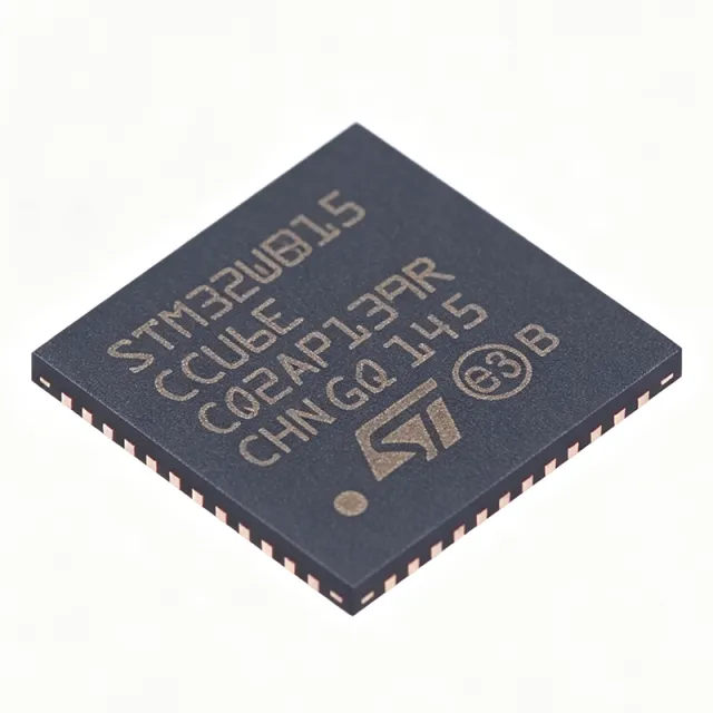
STM32WB15CCU6 - 2.4GHz BLE 5.2 Wireless MCU, 320KB Flash | STMicroelectronics
MPN: STM32WB15CCU6 ✓ Active| Qty | Unit Price | Extended |
|---|---|---|
| 1 | $7.0909 | $7.09 |
| 10 | $5.1212 | $51.21 |
| 100 | $4.5303 | $453.03 |
| 500 | $4.3333 | $2,166.65 |
| 1,000 | $4.1364 | $4,136.40 |
Drop-in alternatives for STM32WB15CCU6 — same package, pin-to-pin compatible. Different-package parts requiring PCB rework are excluded.
Quick Comparison Tool — Select alternative parts for side-by-side comparison:
STM32WB15CCU7
📋 Reference alternative (not in catalog)
STM32WB55CCU6
📋 Reference alternative (not in catalog)
STM32WB55CCU7
📋 Reference alternative (not in catalog)
nRF52832
📋 Reference alternative (not in catalog)
nRF52840
📋 Reference alternative (not in catalog)
STM32WB15CCU6 Maximum Ratings & Electrical Characteristics
| Core | Arm Cortex-M4 + Cortex-M0+ |
| Max Core Frequency | 64 MHz (M4) / 32 MHz (M0+) |
| Flash Memory | 320 KB |
| SRAM | 48 KB |
| Bluetooth Version | Bluetooth Low Energy 5.2 |
| Radio Frequency | 2.4 GHz |
| Max Transmit Power | +6 dBm |
| Receiver Sensitivity | -96 dBm |
| Supply Voltage Range | 1.71 V to 3.6 V |
| Operating Temperature Range | -40°C to +105°C |
| Package | UFQFPN-48 (7x7 mm) |
| Mounting Type | Surface Mount |
| Standby Current | 1.6 µA |
| ADC Resolution | 12-bit |
| Security | AES-128, AES-256, TRNG, 96-bit unique ID |
| RoHS Status | Compliant |
STM32WB15CCU6 Pin Configuration
| Pin 1 | VDD — Power supply (1.71V-3.6V) |
| Pin 2 | PA0 — GPIO / ADC input |
| Pin 3 | PA1 — GPIO / ADC input |
| Pin 4 | PA2 — GPIO / USART2_TX |
| Pin 5 | PA3 — GPIO / USART2_RX |
| Pin 6 | PA4 — GPIO / SPI1_NSS |
| Pin 7 | PA5 — GPIO / SPI1_SCK |
| Pin 8 | PA6 — GPIO / SPI1_MISO |
| Pin 9 | PA7 — GPIO / SPI1_MOSI |
| Pin 10 | PA8 — GPIO / I2C1_SCL |
| Pin 11 | PA9 — GPIO / I2C1_SDA |
| Pin 12 | PA10 — GPIO / USART1_TX |
| Pin 13 | PA11 — GPIO / USART1_RX |
| Pin 14 | PA12 — GPIO / USB_DM |
| Pin 15 | PA13 — GPIO / SWDIO |
| Pin 16 | PA14 — GPIO / SWCLK |
| Pin 17 | PA15 — GPIO / JTDI |
| Pin 18 | PB0 — GPIO / ADC input |
| Pin 19 | PB1 — GPIO / ADC input |
| Pin 20 | PB2 — GPIO / BOOT1 |
| Pin 21 | PB3 — GPIO / JTDO |
| Pin 22 | PB4 — GPIO / JNTRST |
| Pin 23 | PB5 — GPIO / I2C1_SMBA |
| Pin 24 | PB6 — GPIO / I2C1_SCL |
| Pin 25 | PB7 — GPIO / I2C1_SDA |
| Pin 26 | PB8 — GPIO / I2C1_SCL |
| Pin 27 | PB9 — GPIO / I2C1_SDA |
| Pin 28 | PB10 — GPIO / I2C2_SCL |
| Pin 29 | PB11 — GPIO / I2C2_SDA |
| Pin 30 | PB12 — GPIO / SPI2_NSS |
| Pin 31 | PB13 — GPIO / SPI2_SCK |
| Pin 32 | PB14 — GPIO / SPI2_MISO |
| Pin 33 | PB15 — GPIO / SPI2_MOSI |
| Pin 34 | VDD — Power supply |
| Pin 35 | VSS — Ground |
| Pin 36 | PC14 — GPIO / OSC32_IN |
| Pin 37 | PC15 — GPIO / OSC32_OUT |
| Pin 38 | PH0 — OSC_IN (32 MHz crystal) |
| Pin 39 | PH1 — OSC_OUT (32 MHz crystal) |
| Pin 40 | NRST — Reset (active low) |
| Pin 41 | VDDA — Analog power supply |
| Pin 42 | VSSA — Analog ground |
| Pin 43 | VREF+ — ADC reference voltage |
| Pin 44 | VREF- — ADC reference ground |
| Pin 45 | PC0 — GPIO / ADC input |
| Pin 46 | PC1 — GPIO / ADC input |
| Pin 47 | PC2 — GPIO / ADC input |
| Pin 48 | PC3 — GPIO / ADC input |
Safe Operating Area (SOA) & Thermal Characteristics
No official SOA curve available for this digital IC. Always operate within absolute maximum ratings specified in the datasheet. Ensure adequate cooling and derate as needed.
Typical Applications
STM32WB15CCU6 is suitable for 6 applications: Smart Home Devices, Healthcare Wearables, Industrial Wireless Sensor Networks, Asset Tracking, Beacons and Proximity Marketing, Connected Lighting.
Smart Home Devices
The STM32WB15CCU6 is ideal for smart home devices such as smart locks, sensors, and lighting controls. Its low power consumption (1.6 µA standby) and robust BLE 5.2 radio enable battery-powered operation for years. The dual-core architecture allows the Cortex-M0+ to handle the BLE stack while the Cortex-M4 runs application logic, ensuring responsive control. With a transmit power of +6 dBm and receiver sensitivity of -96 dBm, it provides reliable connectivity throughout a typical home. The 320 KB flash supports complex firmware including Over-The-Air (OTA) updates, while the 48 KB SRAM handles real-time data processing. The wide supply voltage range (1.71V-3.6V) allows direct battery connection, simplifying power design. Security features like AES-128/256 encryption and a true random number generator protect smart home communications.
Recommended
Healthcare Wearables
The STM32WB15CCU6 is well-suited for healthcare wearables like fitness trackers and heart rate monitors. Its ultra-low power consumption (1.6 µA standby) extends battery life, critical for continuous health monitoring. The BLE 5.2 radio efficiently transmits health data to smartphones, with +6 dBm TX power ensuring reliable data transfer. The dual-core architecture enables simultaneous sensor data processing and wireless communication without performance degradation. The 12-bit ADC accurately reads analog sensor outputs, while the 320 KB flash stores firmware and health logs. The -40°C to +105°C operating range ensures reliable operation in various environmental conditions. Security features like AES encryption protect sensitive health data during transmission. The compact UFQFPN-48 package (7x7 mm) fits into small wearable form factors.
Recommended
Industrial Wireless Sensor Networks
The STM32WB15CCU6 excels in industrial wireless sensor networks, monitoring temperature, vibration, and pressure in factories. Its wide operating temperature range (-40°C to +105°C) suits harsh industrial environments. The robust BLE 5.2 radio with -96 dBm sensitivity ensures reliable data transmission in noisy RF environments. The dual-core architecture allows real-time sensor data processing on the Cortex-M4 while the Cortex-M0+ manages the wireless stack, ensuring deterministic performance. The 12-bit ADC interfaces with various industrial sensors, and the multiple UART/SPI/I2C interfaces connect to external sensors and actuators. The 1.6 µA standby current enables long battery life for remote sensors. Security features like AES-256 encryption protect industrial data from unauthorized access. The 320 KB flash supports complex industrial protocols and data logging.
Recommended
Asset Tracking
The STM32WB15CCU6 is perfect for asset tracking applications, providing real-time location and status monitoring. Its low power consumption (1.6 µA standby) allows battery-powered trackers to operate for months or years. The BLE 5.2 radio with +6 dBm TX power enables communication with gateways or smartphones over significant distances. The dual-core architecture efficiently handles location algorithms on the Cortex-M4 while the Cortex-M0+ manages BLE advertising and connections. The 320 KB flash stores tracking data and firmware, while the 48 KB SRAM buffers real-time location updates. The wide supply voltage range (1.71V-3.6V) supports various battery chemistries. Security features like AES encryption protect location data from unauthorized access. The compact UFQFPN-48 package enables small, unobtrusive tracker designs.
Recommended
Beacons and Proximity Marketing
The STM32WB15CCU6 is an excellent choice for BLE beacons used in proximity marketing and indoor navigation. Its BLE 5.2 radio supports advertising extensions, enabling longer-range beacon broadcasts. The +6 dBm TX power provides configurable range from a few meters to over 100 meters, allowing precise proximity detection. The ultra-low power consumption (1.6 µA standby) ensures beacon batteries last for years. The dual-core architecture allows the Cortex-M0+ to handle advertising while the Cortex-M4 manages sensor data or configuration. The 320 KB flash stores beacon configuration and firmware updates. The wide supply voltage range supports coin cell batteries (1.71V-3.6V). Security features prevent unauthorized beacon configuration changes. The compact UFQFPN-48 package fits into small beacon housings.
Recommended
Connected Lighting
The STM32WB15CCU6 is ideal for connected lighting systems, enabling smart control of LED lights via BLE. Its BLE 5.2 radio supports mesh networking, allowing lights to relay commands and create large-scale lighting networks. The +6 dBm TX power ensures reliable communication between lights and controllers. The dual-core architecture handles lighting control algorithms on the Cortex-M4 while the Cortex-M0+ manages the wireless stack. The 12-bit ADC can monitor current and voltage for diagnostics. The 320 KB flash supports complex lighting scenes and firmware updates. The wide supply voltage range (1.71V-3.6V) allows direct connection to lighting power supplies. Security features like AES encryption prevent unauthorized control. The -40°C to +105°C operating range suits various lighting environments.
Recommended
Recommended Products Summary
Engineering reference data for STM32WB15CCU6 — comparison, design guidance, and compliance information.
Selection Guide
Comparison with Alternatives
| Parameter | This Product | STM32WB15CCU7 | STM32WB55CCU6 | nRF52832 |
|---|---|---|---|---|
| Package | UFQFPN-48 (7x7 mm) | UFQFPN-48 (7x7 mm) - same | UFQFPN-48 (7x7 mm) - same | QFN-48 (6x6 mm) - different |
| Brand | STMicroelectronics | STMicroelectronics | STMicroelectronics | Nordic Semiconductor |
| Flash Memory | 320 KB | 512 KB | 1 MB | 512 KB |
| SRAM | 48 KB | 64 KB | 256 KB | 64 KB |
| Max Core Frequency | 64 MHz (M4) / 32 MHz (M0+) | 64 MHz (M4) / 32 MHz (M0+) | 64 MHz (M4) / 32 MHz (M0+) | 64 MHz (M4) |
| Bluetooth Version | BLE 5.2 | BLE 5.2 | BLE 5.2 | BLE 5.2 |
| Max Transmit Power | +6 dBm | +6 dBm | +6 dBm | +4 dBm |
| Receiver Sensitivity | -96 dBm | -96 dBm | -96 dBm | -96 dBm |
| Standby Current | 1.6 µA | 1.6 µA | 1.6 µA | 1.9 µA |
| Supply Voltage Range | 1.71V - 3.6V | 1.71V - 3.6V | 1.71V - 3.6V | 1.7V - 3.6V |
Key Differentiators
- Dual-core architecture with dedicated radio processor (vs nRF52832)
- Higher transmit power (vs nRF52832)
- Lower standby current (vs nRF52832)
Design Notes
For optimal RF performance, place the 2.4 GHz antenna on the edge of the PCB with a 50-ohm impedance-controlled trace. Keep the antenna away from ground planes and other components. Use a ground plane on the layer below the antenna for proper radiation. Follow ST's application note AN5129 for detailed antenna design guidelines.
Decouple the VDD pins with a 100 nF ceramic capacitor placed as close as possible to each pin, and a 4.7 µF bulk capacitor for the main supply. For the VDDA pin, use a 1 µF capacitor and a ferrite bead to isolate analog noise. Ensure the supply voltage stays within 1.71V-3.6V, including during BLE transmission current spikes.
Place the 32 MHz crystal and its load capacitors close to the PH0/PH1 pins, with short traces to minimize parasitic capacitance. Similarly, place the 32.768 kHz crystal near PC14/PC15. Keep these traces away from high-speed digital signals to avoid interference. Use ground vias around the crystal area to shield it.
Compliance Information
RoHS compliant per STMicroelectronics product page. Not AEC-Q100 qualified - this is a consumer/industrial grade device.