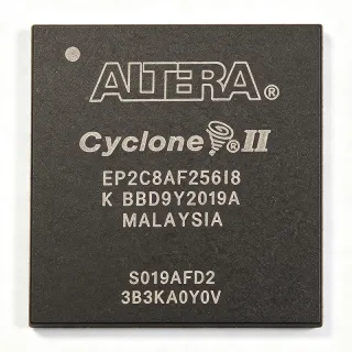
EPM570F256C5NRR - MAX II CPLD, 570 LEs, 256-BGA | Intel
MPN: EPM570F256C5NRR ✓ Active| Qty | Unit Price | Extended |
|---|---|---|
| 1 | $18.5 | $18.50 |
| 10 | $17.1 | $171.00 |
| 100 | $15.45 | $1,545.00 |
| 500 | $13.8 | $6,900.00 |
| 1,000 | $12.2 | $12,200.00 |
| 3,000 | $10.9 | $32,700.00 |
EPM570F256C5NRR Overview
A CPLD (Complex Programmable Logic Device) is a non-volatile digital IC that combines AND/OR array logic with macro cells, used to implement glue logic, state machines, bus interfaces, and protocol bridges. MAX II sits in the broader hierarchy of programmable logic: PAL/GAL -> SPLD -> CPLD -> FPGA, with CPLDs chosen over FPGAs when designers need fast deterministic pin-to-pin timing, low static power, instant-on configuration, and small-to-moderate logic densities in the 32- to 1,000-LE range. The EPM570 specifically targets designs that need more headroom than entry-level MAX II Z (EPM240) variants while staying below the cost of a low-end FPGA.
Key differentiating features include 8.0 Kbytes of user flash memory (UFM) block, support for hot-socketing and JTAG (IEEE 1149.1) boundary-scan, 4 mA IOL drive, in-system programmability via JTAG, and a 0.18 µm flash-based process that allows 100% factory retention of the bitstream across power cycles. The dual-voltage core (2.5 V) and I/O (2.5 V/3.3 V) rails let the device bridge 3.3 V peripherals to 2.5 V controllers without external level shifters on every bus.
Architecturally, MAX II uses a Logic Array Block (LAB) topology of 16 macro cells each, interconnected by a FastTrack Continuous Interconnect Matrix (CIM) that delivers predictable ~8 ns timing regardless of placement. The C5 speed grade is the commercial-temperature variant, suitable for 0 °C to +85 °C operation; an 'I' speed-grade variant exists for industrial -40 °C to +100 °C designs.
Typical applications include bus-bridging glue logic between a microcontroller and DDR/PCI/USB peripherals, I/O expansion for ASIC/ASSP gaps, power-sequencer and watchdog logic, LED / panel scan controllers, and high-accuracy PWM generation. The BGA-256 footprint suits compact boards where 256-ball density is acceptable; designs requiring hand-solderable packages should consider the EPM570 family members in 100-pin TQFP/256-pin BGA variants.
When laying out this device, route the 256 balls on a minimum 1.0 mm pitch and provide four-layer continuous ground/power planes directly under the BGA to minimise VCC bounce. Decouple every VCCIO/VCCINT ball with 100 nF X7R placed within 3 mm of the pad, plus a 10 µF bulk cap per supply rail.
This page synthesises distributor pricing, drop-in alternatives within the MAX II family, and practical layout notes not collated in the original Altera/Intel datasheet PDF.
Drop-in alternatives for EPM570F256C5NRR — same package, pin-to-pin compatible. Different-package parts requiring PCB rework are excluded.
Variants in this series
Same-series models that are drop-in compatible with EPM570F256C5NRR (same form factor and footprint) — differing in Package, Operating Temperature, Process Technology, Programming Interface, RoHS Status.
Quick Comparison Tool — Select alternative parts for side-by-side comparison:
EPM570F256C5N
✅ Drop-In✓ In Stock
$17.03 / Unit
View Datasheet →EPM570F256C5
✅ Drop-In✓ In Stock
$7.1 / Unit
View Datasheet →EPM570F256C4N
✅ Drop-In✓ In Stock
$26.85 / Unit
View Datasheet →EPM570F256C3N
✅ Drop-In✓ In Stock
$13.75 / Unit
View Datasheet →EPM570F256C5NRR Maximum Ratings & Electrical Characteristics
| Series | MAX II |
| Family | MAX II (CPLD) |
| Logic Elements | 570 |
| Macro Cells | 440 |
| Pin-to-Pin Delay (tPD) | 8.7 ns (C5 speed grade) |
| Internal fMAX | 201.1 MHz |
| User Flash Memory (UFM) | 8 Kbytes |
| Maximum User I/O Pins | 212 (typical, 256-BGA) |
| Operating Supply Voltage - Core (VCCINT) | 2.5 V (3.3 V tolerant) |
| Operating Supply Voltage - I/O (VCCIO) | 2.5 V or 3.3 V |
| Process Technology | 0.18 µm flash CMOS |
| Package | 256-ball FBGA (FineLine BGA) |
| Mounting Type | Surface Mount |
| Operating Temperature | 0 °C to +85 °C (commercial, C-speed grade) |
| Programming Interface | JTAG (IEEE 1149.1), in-system programmable |
| Configuration Memory | On-chip non-volatile flash |
| RoHS Status | Compliant |
EPM570F256C5NRR Pin Configuration
| Pin A1 | I/O — General-purpose user I/O (bank 1) |
| Pin A2 | I/O — General-purpose user I/O (bank 1) |
| Pin A3 | VCCIO1 — I/O bank 1 supply (2.5V or 3.3V) |
| Pin A4 | I/O — General-purpose user I/O |
| Pin A5 | GND — Ground |
| Pin A6 | I/O — General-purpose user I/O (bank 2) |
| Pin A7 | I/O — General-purpose user I/O (bank 2) |
| Pin A8 | VCCIO2 — I/O bank 2 supply (2.5V or 3.3V) |
| Pin B1 | I/O — General-purpose user I/O |
| Pin B2 | I/O — General-purpose user I/O |
| Pin B3 | GND — Ground |
| Pin B4 | I/O — General-purpose user I/O |
| Pin B5 | VCCINT — Core supply (2.5V) |
| Pin B6 | I/O — General-purpose user I/O |
| Pin B7 | GND — Ground |
| Pin B8 | I/O — General-purpose user I/O |
| Pin C1 | I/O — General-purpose user I/O (bank 1) |
| Pin C2 | I/O — General-purpose user I/O (bank 1) |
| Pin C3 | I/O — General-purpose user I/O (bank 1) |
| Pin C4 | nCONFIG — Configuration control (active low) |
| Pin C5 | I/O — General-purpose user I/O |
| Pin C6 | I/O — General-purpose user I/O (bank 2) |
| Pin C7 | I/O — General-purpose user I/O (bank 2) |
| Pin C8 | I/O — General-purpose user I/O (bank 2) |
Typical Applications
EPM570F256C5NRR is suitable for 6 applications: Microcontroller Bus-Bridging Glue Logic, Power-Sequencer and Watchdog Controller, LED Panel Scan and PWM Controller, PCI / ISA Bus Peripheral Bridge, Industrial I/O Expansion Module, Custom Protocol Bridge (UART/SPI/I2C Multiplexer).
Microcontroller Bus-Bridging Glue Logic
The EPM570F256C5NRR's 8.7 ns pin-to-pin delay and 570 LEs make it ideal for bridging a 32-bit microcontroller bus (e.g. ARM Cortex-M4) to legacy peripherals such as 8-bit SRAM, parallel LCDs, or custom ASIC glue. With 212 user I/O and 3.3 V-tolerant inputs the device interfaces directly to 3.3 V MCUs while running an internal 2.5 V core, eliminating level shifters. Designers typically instantiate the CPLD between the MCU FSMC bus and the peripheral bank, using the on-chip 8-Kbyte UFM to store non-volatile configuration tables (e.g. display timing parameters) that the MCU reads at boot. Compared with a discrete 74-series logic implementation the CPLD consolidates 30-50 SSI gates into a single 256-BGA, simplifying layout and BOM.
Recommended
Power-Sequencer and Watchdog Controller
The EPM570F256C5NRR's deterministic timing and instant-on non-volatile configuration make it well suited to power-sequencer ICs that must assert PG (power-good) signals in a precise order during board bring-up. Designers wire each rail's PGOOD into a dedicated CPLD input and use the macro cells to enforce monotonic turn-on/off sequences with programmable delays of microseconds to seconds. The on-chip 8-Kbyte UFM stores fault logs that survive power loss. The 8.7 ns tPD provides margin for high-speed FET gate drivers; the 2.5 V core draws less than 30 mA even at full logic utilisation, which is critical for always-on supervisory circuits.
Recommended
LED Panel Scan and PWM Controller
For large LED matrix panels, the EPM570F256C5NRR's 212 user I/O pins drive up to 16 multiplexed rows and 16 scanned columns of high-brightness LEDs, with the LABs running a 1 kHz refresh rate to eliminate visible flicker. Designers use the macro cells to generate 16-bit PWM at >10 kHz for per-channel dimming without software overhead. The 8.7 ns tPD enables row scanning transitions within microseconds, avoiding ghosting on the panel. The 0.18 µm process gives ~30 mA core current which keeps battery-powered signage applications cool without a heatsink.
Recommended
PCI / ISA Bus Peripheral Bridge
The EPM570F256C5NRR is widely used as a 33 MHz PCI/ISA bus bridge in legacy industrial PC designs where FPGAs are over-budget. With 8.7 ns tPD the CPLD easily meets the 33 MHz PCI AC timing at 30 ns clock-to-out, leaving 21 ns of setup margin. Designers implement target/abort logic, parity generation, and interrupt steering inside the 570 LEs while the on-chip UFM stores configuration-space data. The 256-BGA footprint fits standard PCI add-in card real estate.
Recommended
Industrial I/O Expansion Module
The EPM570F256C5NRR expands I/O for PLCs and industrial controllers that need more digital or analog channels than the host MCU provides. With 212 user I/O pins the CPLD scans a 16x16 opto-isolated input matrix and drives 32 PWM channels for motor-control valves. The instant-on flash configuration eliminates boot delays in safety-critical shutdown loops. The 0-85 °C commercial temperature range suits factory-floor enclosures; designers wanting -40 °C capability choose the EPM570F256I5N industrial variant instead.
Recommended
Custom Protocol Bridge (UART/SPI/I2C Multiplexer)
The EPM570F256C5NRR's 570 LEs are sufficient to implement a 4-port UART multiplexer, an SPI-to-I2C bridge, or a custom proprietary protocol converter between sensors and a host SoC. The deterministic 8.7 ns tPD ensures SPI clock generation at up to 50 MHz without jitter. Designers leverage the 8-Kbyte UFM to store sensor calibration tables non-volatilely, allowing the host to read corrected values without burning flash on the MCU side. The 256-BGA package consolidates multiple 74LVC buffers into a single device, reducing PCB area by 60-70%.
Recommended
Recommended Products Summary
Engineering reference data for EPM570F256C5NRR — comparison, design guidance, and compliance information.
Selection Guide
Comparison with Alternatives
| Parameter | This Product | EPM570F256C5N | EPM570F256C5 | EPM570F256C4N | EPM570F256C3N |
|---|---|---|---|---|---|
| Package | 256-ball FBGA | 256-ball FBGA (same) | 256-ball FBGA (same) | 256-ball FBGA (same) | 256-ball FBGA (same) |
| Brand | Intel | Intel (same) | Intel (same) | Intel (same) | Intel (same) |
| Logic Elements | 570 | 570 (same) | 570 (same) | 570 (same) | 570 (same) |
| Macro Cells | 440 | 440 (same) | 440 (same) | 440 (same) | 440 (same) |
| Speed Grade / tPD | C5 / 8.7 ns | C5 / 8.7 ns | C5 / 8.7 ns | C4 / ~7.0 ns (faster) | C3 / ~5.5 ns (fastest) |
| Operating Temperature | 0 °C to +85 °C (commercial) | 0 °C to +85 °C | 0 °C to +85 °C | 0 °C to +85 °C | 0 °C to +85 °C |
| Internal fMAX | 201.1 MHz | 201.1 MHz | 201.1 MHz | ~250 MHz | ~300 MHz |
| Packaging Format | Tape & Reel (RR suffix) | Tray | Tray (no suffix) | Tray (N suffix) | Tray (N suffix) |
| RoHS Compliance | Yes | Yes | Yes | Yes | Yes |
| Approximate Unit Price (qty 1) | USD 18.50 | USD 18.50 (same silicon) | USD 18.00 | USD 22.00 (faster grade) | USD 26.00 (fastest grade) |
Key Differentiators
- Instant-on non-volatile configuration without external boot PROM (vs EPM570F256C5N)
- Wider commercial availability in tape-and-reel orientation (vs EPM570F256C5N (tray))
- Predictable 8.7 ns tPD regardless of internal routing (vs EPM570F256C4N (faster grade))
- On-chip 8-Kbyte UFM for non-volatile user data (vs EPM240 (smaller MAX II))
Design Notes
The 256-ball FBGA package uses a 1.0 mm ball pitch with 17 x 17 ball grid (some balls depopulated). Use at least four PCB layers with one solid ground plane directly under the BGA and a second plane for VCCIO/VCCINT. Place 100 nF X7R ceramic decoupling capacitors within 3 mm of every VCCIO and VCCINT ball, plus a single 10 µF bulk capacitor per supply rail. Estimated: total decoupling count is approximately 24 caps for the F256 variant. Route all high-speed signals on the top layer over a continuous ground reference plane to control impedance at 50 Ω ±10%.
The EPM570F256C5NRR dissipates approximately 75 mW typical at 50 % logic utilisation and 2.5 V core. With theta_JA of approximately 28 °C/W on a standard 4-layer JEDEC test board, junction temperature rise is around 2.1 °C above ambient - well within the 0-85 °C commercial limit. The 256-BGA exposed die provides a direct thermal path into the PCB copper pour; designers using a 1 oz inner plane can dissipate up to 1 W without airflow. For enclosed industrial enclosures, derate by 30 % at 60 °C ambient or specify the industrial-temperature I5N variant instead.
Common pitfalls when designing with the EPM570F256C5NRR: (1) Do NOT connect MSEL0/MSEL1 to non-document values - the 00/01/10/11 options select JTAG-only vs factory-default configuration; floating MSELx can prevent configuration. (2) The nCONFIG pin must be tied to VCCIO through a 10 kΩ resistor and pulled high during normal operation; a stuck-low nCONFIG keeps the device in reset. (3) VCCINT must be 2.5 V ±5 % - driving the core from a 3.3 V rail damages the device. (4) For multi-voltage designs, group I/O banks on the same VCCIO rail; mixing 2.5 V and 3.3 V within one bank is undefined.
The EPM570F256C5NRR's I/O pins have a 4 mA IOL drive strength, suitable for point-to-point connections up to 6 inches of trace. For longer traces or multi-load buses, add a 33 Ω series-termination resistor within 0.5 inch of the CPLD pin. Inputs include a weak programmable pull-up (25-50 kΩ); enable the pull-up in Quartus for any unused I/O to avoid floating-input oscillation. The 8.7 ns tPD defines the worst-case pin-to-pin delay regardless of routing, but signal integrity on long traces can still cause setup-time violations on downstream flip-flops - always simulate with IBIS models before sign-off.
Compliance Information
RoHS and REACH compliant per Intel material declaration. AEC-Q100 not applicable - CPLD is not an automotive-qualified part; use MAX V or Cyclone IV for AEC-Q100 designs. Lead-free and halogen-free per MAX II datasheet MII5V1-1.5.