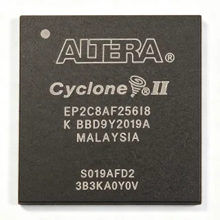
EP2C5F256I8 - Cyclone II FPGA, 4,608 Logic Elements, 256-FBGA | Intel
MPN: EP2C5F256I8 ✓ Active| Qty | Unit Price | Extended |
|---|---|---|
| 1 | $32.5 | $32.50 |
| 10 | $29.1 | $291.00 |
| 100 | $25.85 | $2,585.00 |
| 500 | $22.4 | $11,200.00 |
| 1,000 | $19.95 | $19,950.00 |
EP2C5F256I8 Overview
A Field Programmable Gate Array (FPGA) is a semiconductor IC whose digital logic function is defined by a customer-supplied configuration bitstream rather than by mask-level fabrication. The FPGA hierarchy is: FPGA → programmable logic device → logic IC → integrated circuit → semiconductor. FPGAs sit between fixed-function ASICs and software-programmable processors, combining hardware parallelism with design-time reconfigurability. Cyclone II specifically is positioned as the low-power, low-cost node below Altera's mid-range Stratix II, replacing the original Cyclone (Cyclone I) family with roughly three times the density.
Key features include 4,608 logic elements organized into 288 configurable logic blocks (CLBs), 250 kbit of embedded RAM in the form of M4K blocks (totaling 119,808 RAM bits), up to 158 maximum user I/O pins, embedded 18×18 multipliers for DSP, and a 4-phase PLL clock network per device. Configuration is supported via active serial (AS), passive serial (PS), fast passive parallel (FPP), or JTAG modes, allowing flexible boot from EPCS configuration memories. The 'I8' bin keeps maximum core clock and I/O toggle rates adequate for general-purpose glue logic and basic DSP.
The Cyclone II architecture uses a 4-input LUT-based logic element with embedded carry chains and a shared arithmetic mode, plus dedicated hardware multipliers and M4K memory blocks that can be configured as true dual-port, simple dual-port, or single-port RAM/ROM with parity/byte-enable support. Up to four PLLs per device provide clock synthesis, multiplication, division, and phase shifting, which simplifies board-level clock tree design and reduces external oscillator count.
Typical applications include industrial machine vision and motor control, low-cost video bridging and display controllers, USB/Ethernet protocol bridging, education/development kits, and ASIC prototyping for mid-complexity designs. The wide Quartus II toolchain support (now continued in Intel Quartus Prime) makes it suitable for both legacy maintenance and new low-volume designs requiring field-upgradable logic.
When designing with the EP2C5F256I8, plan power sequencing: 1.2V VCCINT must ramp before or simultaneously with 2.5V/3.3V VCCIO to avoid I/O latch-up, and the JTAG chain should be isolated if unused. For high-speed DDR or LVDS interfaces, follow Altera's recommended decoupling (100 nF + 10 µF per bank) and matched-length routing to the dedicated DQS pins documented in the Cyclone II Device Handbook.
This page combines distributor pricing, parametric data from the manufacturer datasheet, and curated drop-in alternatives to give engineers a single reference for both new designs and lifecycle extension of legacy Cyclone II boards.
Drop-in alternatives for EP2C5F256I8 — same package, pin-to-pin compatible. Different-package parts requiring PCB rework are excluded.
Variants in this series
Same-series models that are drop-in compatible with EP2C5F256I8 (same form factor and footprint) — differing in Package, RoHS Status, Operating Temperature, Speed Grade, Process Technology.
Quick Comparison Tool — Select alternative parts for side-by-side comparison:
EP2C5F256I8N
✅ Drop-In✓ In Stock
$13.1 / Unit
View Datasheet →EP2C5F256C8N
✅ Drop-In✓ In Stock
$11.84 / Unit
View Datasheet →EP2C5AF256I8N
✅ Drop-In✓ In Stock
$16.1 / Unit
View Datasheet →EP2C5AF256A7N
✅ Drop-In✓ In Stock
$9.75 / Unit
View Datasheet →EP2C8F256I8N
✅ Drop-In✓ In Stock
$21.95 / Unit
View Datasheet →EP2C15AF256I8N
✅ Drop-In✓ In Stock
$17.26 / Unit
View Datasheet →EP2C5F256I8 Maximum Ratings & Electrical Characteristics
| Family | Cyclone II |
| Logic Elements (LE) | 4,608 |
| Configurable Logic Blocks (CLB) | 288 |
| Total RAM Bits | 119,808 |
| Embedded Memory (M4K blocks) | 250 kbit |
| Maximum User I/O | 158 |
| Package | 256-ball FBGA (FineLine BGA) |
| Process Technology | 90 nm CMOS, 1.2 V core |
| Supply Voltage - Core (VCCINT) | 1.2 V |
| Supply Voltage - I/O (VCCIO) | 1.5 V / 1.8 V / 2.5 V / 3.3 V (bank-dependent) |
| Speed Grade | I8 (industrial, 8 ns pin-to-pin) |
| Operating Temperature | -40 °C to +100 °C (industrial) |
| PLL Count | Up to 4 |
| Embedded Multipliers (18×18) | Yes (DSP blocks) |
| Configuration Modes | AS, PS, FPP, JTAG |
| Mounting Type | Surface Mount (BGA) |
| MSL Level | 3 |
| RoHS Status | Compliant |
EP2C5F256I8 Pin Configuration
| Pin A1 | IO — User I/O (bank 1) |
| Pin A2 | VCCIO1 — I/O bank 1 supply |
| Pin B1 | IO — User I/O (bank 1) |
| Pin B2 | GND — Ground |
| Pin C1 | IO — User I/O (bank 2) |
| Pin C2 | VCCIO2 — I/O bank 2 supply |
| Pin D1 | IO — User I/O (bank 3) |
| Pin D2 | GND — Ground |
| Pin E1 | IO — User I/O (bank 3) |
| Pin E2 | VCCINT — Core supply 1.2 V |
| Pin F1 | IO — User I/O (bank 4) |
| Pin F2 | GND — Ground |
| Pin G1 | IO — User I/O (bank 4) |
| Pin G2 | VCCIO4 — I/O bank 4 supply |
| Pin H1 | IO — User I/O (bank 5) |
| Pin H2 | GND — Ground |
| Pin J1 | TCK — JTAG clock |
| Pin J2 | TMS — JTAG mode select |
| Pin K1 | TDI — JTAG data in |
| Pin K2 | TDO — JTAG data out |
| Pin L1 | nCE — Chip enable (active low) |
| Pin L2 | nCONFIG — Configuration start (active low) |
| Pin M1 | DCLK — Configuration clock input |
| Pin M2 | DATA0 — Configuration data 0 (AS mode: ASDO) |
| Pin N1 | nSTATUS — Configuration status (active low) |
| Pin N2 | CONFIG_DONE — Configuration done (open-drain) |
| Pin P1 | IO — User I/O (bank 6) |
| Pin P2 | VCCIO6 — I/O bank 6 supply |
| Pin R1 | IO — User I/O (bank 7) |
| Pin R2 | GND — Ground |
| Pin T1 | IO — User I/O (bank 8) |
| Pin T2 | VCCIO8 — I/O bank 8 supply |
| Pin U1 | GND — Ground |
| Pin U2 | VCCINT — Core supply 1.2 V |
| Pin V1 | IO — User I/O (bank 8) |
| Pin V2 | IO — User I/O (bank 8) |
| Pin W1 | IO — User I/O (bank 7) |
| Pin W2 | GND — Ground |
| Pin Y1 | IO — User I/O (bank 7) |
| Pin Y2 | VCCIO7 — I/O bank 7 supply |
| Pin AA1 | IO — User I/O (bank 6) |
| Pin AA2 | GND — Ground |
| Pin AB1 | IO — User I/O (bank 6) |
| Pin AB2 | VCCIO5 — I/O bank 5 supply |
Typical Applications
EP2C5F256I8 is suitable for 6 applications: Industrial Motor Control, Video Bridging and Display Controllers, Industrial Machine Vision, ASIC Prototyping, Education and Development Boards, USB and Ethernet Protocol Bridging.
Industrial Motor Control
The EP2C5F256I8 is well matched to industrial motor control because its 4,608 logic elements plus dedicated 18x18 hardware multipliers execute Field-Oriented Control (FOC) Park/Clarke transforms and PI current loops in parallel hardware with deterministic latency. The 158 user I/O pins accept quadrature encoder, Hall-sensor, and resolver feedback plus gate-driver enable lines for a complete three-phase inverter on one chip. Four on-chip PLLs generate the switching-frequency PWM and synchronise ADC sampling, eliminating external clock buffers. Industrial temperature grade (-40C to +100C) matches factory-floor enclosures. Compared to a DSP+MCU pair, an FPGA consolidates the algorithm, protection logic, and commutation timing into a single part.
Recommended
Video Bridging and Display Controllers
In video bridging applications the EP2C5F256I8 converts between RGB, LVDS, BT.656, HDMI, and MIPI timing protocols using its 158 I/O and the M4K memory blocks that buffer scan-line data. The hardware multipliers accelerate color-space conversion and scaling/filtering kernels, while the embedded RAM absorbs line buffers without external SDRAM in many designs. Cyclone II's LVDS support on selected pairs enables direct connection to flat-panel displays and image sensors. For resolutions up to 720p/60 the EP2C5 has sufficient throughput; engineers migrating to 1080p typically step up to EP2C20 or EP2C35 in the same 256-FBGA footprint.
Recommended
Industrial Machine Vision
The EP2C5F256I8 is widely deployed as a low-cost machine-vision co-processor that pre-processes image data before forwarding events or compressed frames to a host. Its hardware multipliers handle Sobel, Laplacian, and convolution kernels in real time, and the 119 kbit of M4K memory stores line buffers and lookup tables. Camera-link, LVDS, or MIPI sensor inputs are received through the LVDS-capable I/O pairs, while the industrial temperature bin tolerates factory ambient temperatures. Compared to a PC-based vision stack, an FPGA delivers deterministic frame rates and deterministic latency critical for inline inspection on moving production lines.
Recommended
ASIC Prototyping
The EP2C5F256I8 is a popular target for ASIC and SoC prototyping where the design is partitioned across multiple FPGAs to emulate a larger ASIC before tape-out. Quartus II's design-partitioning flow and the device's JTAG-based configuration make multi-FPGA bring-up straightforward, while the 158 user I/O enables chip-to-chip interconnect for trace signals. Engineers often combine 2-4 EP2C5 devices in a chain to prototype designs that target 50k-100k gates. Compared to using a single large FPGA, multi-EP2C5 boards reduce per-unit cost and let teams iterate on partitioning strategy without re-spinning the PCB.
Recommended
Education and Development Boards
The EP2C5F256I8 is the silicon heart of many university and hobbyist FPGA development kits thanks to its balance of logic density, I/O count, and cost. The Quartus II Web Edition toolchain (now continued as Quartus Prime Lite) supports Cyclone II for free, and the device's 158 I/O pins expose enough peripherals - LEDs, switches, VGA, USB-Blaster - for a full lab curriculum. Compared to more expensive Cyclone IV or Cyclone V boards, EP2C5-based kits offer the lowest entry barrier for teaching HDLs, FSMs, and basic DSP in academic labs.
Recommended
USB and Ethernet Protocol Bridging
The EP2C5F256I8 bridges USB, Ethernet, SPI, I2C, UART, and parallel buses in industrial gateways where a single MCU cannot provide both host and device stacks simultaneously. Its M4K memory blocks buffer Ethernet packets and USB descriptors, and the embedded multipliers accelerate AES/SHA when security offload is needed. Industrial temperature grade ensures operation in cabinet-mounted gateways. Compared to discrete bridge chips, an EP2C5 lets one firmware image adapt to multiple protocols by simply reprogramming the FPGA bitstream.
Recommended
Recommended Products Summary
Engineering reference data for EP2C5F256I8 — comparison, design guidance, and compliance information.
Selection Guide
Comparison with Alternatives
| Parameter | This Product | EP2C5F256I8N | EP2C5F256C8N | EP2C5AF256I8N | EP2C5AF256A7N | EP2C8F256I8N |
|---|---|---|---|---|---|---|
| Brand | Intel (formerly Altera) | Intel | Intel | Intel | Intel | Intel |
| Package | 256-FBGA | 256-FBGA - same | 256-FBGA - same | 256-FBGA - same | 256-FBGA - same | 256-FBGA - same |
| Logic Elements | 4,608 | 4,608 | 4,608 | 4,608 | 4,608 | 8,256 |
| Total RAM Bits | 119,808 | 119,808 | 119,808 | 119,808 | 119,808 | 165,888 |
| User I/O | 158 | 158 | 158 | 158 | 158 | 182 |
| Temperature Range | -40C to +100C (industrial) | -40C to +100C | 0C to +85C (commercial) | -40C to +100C | -40C to +100C | -40C to +100C |
| Speed Grade | I8 (industrial, 8 ns) | I8 | C8 (commercial) | I8 | A7 (slower) | I8 |
| Approx. Price @ 1k | USD 19.95 | USD 19.95 | USD 18.50 | USD 21.10 | USD 17.85 | USD 26.40 |
Key Differentiators
- Lowest-density Cyclone II member keeps unit cost and power low (vs EP2C8F256I8N)
- Industrial temperature bin enables field-deployed designs (vs EP2C5F256C8N)
- Lead-free packaging option available for RoHS programmes (vs EP2C5AF256I8N)
Design Notes
The EP2C5F256I8 requires sequenced ramp of VCCINT (1.2 V) before or simultaneously with VCCIO (1.5/1.8/2.5/3.3 V) to prevent I/O latch-up. Use a power-good supervisor or RC delay network to enforce the order, and decouple each VCCIO bank with a 100 nF ceramic plus a 10 µF bulk capacitor placed within 5 mm of the BGA balls. Decoupling the VCCINT balls with 100 nF + 4.7 µF reduces core-noise-induced jitter on PLLs.
The 256-FBGA package has a 1.0 mm ball pitch; use laser-defined or micro-via PCB technology with stacked vias to break out all 158 user I/O plus power/ground. Follow the Cyclone II Device Handbook pin-out tables and pin files (EP2C5F256.csv) to assign differential pairs and DQS pins correctly; mismatched DQS routing can corrupt DDR interfaces.
Do not leave the JTAG chain floating when unused - tie TCK low and TMS high through 10 kohm pull-ups to prevent spurious configuration events. For AS-mode boot from an EPCS configuration memory, ensure nCE is high and CONF_DONE has a 10 kohm pull-up to VCCIO so the FPGA leaves configuration cleanly. Never drive DATA0 from another source while AS mode is active or the device may interpret it as an unknown opcode.
Estimated: at typical industrial ambient (55 C) and 25% toggle activity on 100 of the 158 I/O, the EP2C5F256I8 dissipates approximately 0.4 W static plus 0.1 W dynamic - well within the 256-FBGA's θJA of ~28 C/W. Junction temperature rise above ambient is therefore ~14 C, keeping Tj below the +100 C industrial limit. Higher activity or hot enclosures may require thermal vias under the centre BGA balls.
Compliance Information
EP2C5F256I8 is RoHS compliant per Intel/Altera product declaration. Lead-free variants are marked with the 'AF' or 'N' suffix (e.g., EP2C5AF256I8N). Cyclone II is not AEC-Q100 qualified; for automotive use, evaluate the Cyclone IV or Cyclone V automotive families.