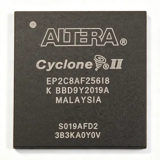
EP2C5F256C7N - Cyclone II FPGA 4,608 LEs 158 I/O FBGA-256 | Intel
MPN: EP2C5F256C7N ✗ End of Life| Qty | Unit Price | Extended |
|---|---|---|
| 1 | $38.5 | $38.50 |
| 10 | $34.2 | $342.00 |
| 100 | $28.9 | $2,890.00 |
| 250 | $26.1 | $6,525.00 |
| 500 | $23.4 | $11,700.00 |
EP2C5F256C7N Overview
A Field-Programmable Gate Array (FPGA) is a semiconductor device built around an array of configurable logic blocks (CLBs), programmable interconnect, and I/O cells that designers can reconfigure after manufacturing to implement arbitrary digital logic, DSP pipelines, or glue logic. FPGAs occupy a tier in the programmable-logic hierarchy between CPLDs (smaller, non-volatile, deterministic timing) and ASICs (largest, lowest unit cost, fixed function); the Cyclone II family specifically targets the low-cost edge of that hierarchy, competing with mid-range microcontrollers and ASSPs on price while delivering hardware-level parallelism.
Key features of the EP2C5F256C7N include 4,608 logic elements, 119,808 RAM bits (organized as M4K memory blocks), up to 158 user I/O pins, two PLLs supporting 16 global clock networks, and JTAG-based configuration via the standard Active Serial (AS), Passive Serial (PS), and JTAG modes. The 90 nm process delivers low static and dynamic power, and the device supports hot-socketing and PCI Express hard IP PIPE compatibility for endpoint applications.
The Cyclone II architecture uses 4-input look-up tables (LUT4) per logic element, true dual-port M4K memory blocks, and dedicated multiplier blocks capable of 18x18 signed multiplication. The PLL macro supports clock multiplication, division, phase shift, and external feedback for precise system-level clock management. The 256-ball FBGA package provides 158 usable I/O across 8 I/O banks, allowing flexible voltage and clock domain partitioning.
Typical applications include industrial motor control, video processing bridges, low-cost DSP front-ends, I/O expansion and protocol bridging, consumer display controllers, and educational/hobbyist development. The combination of low unit cost, mature Quartus II toolchain support, and 158 I/O makes the EP2C5F256C7N a common choice for legacy and cost-sensitive designs.
When designing with this device, plan for a 1.2V core supply plus one or more bank I/O supplies (1.5V, 1.8V, 2.5V, or 3.3V). Decoupling must include 0.1 uF and bulk capacitors on every VCC pin, and JTAG chain length must be analyzed if multiple devices are configured in series. Configuration data should be stored in a serial configuration device (EPCS) for standalone boot.
This page synthesizes distributor pricing, same-family and cross-brand drop-in alternatives, and practical design notes not found in the manufacturer datasheet.
Drop-in alternatives for EP2C5F256C7N — same package, pin-to-pin compatible. Different-package parts requiring PCB rework are excluded.
Variants in this series
Same-series models that are drop-in compatible with EP2C5F256C7N (same form factor and footprint) — differing in Package, Speed Grade, Process Technology, Operating Temperature, Total RAM Bits.
Quick Comparison Tool — Select alternative parts for side-by-side comparison:
EP2C5F256C8N
✅ Drop-In✓ In Stock
$11.84 / Unit
View Datasheet →EP2C5F256C6N
✅ Drop-In✓ In Stock
$11.4 / Unit
View Datasheet →EP2C5F256C7
✅ Drop-In✓ In Stock
$16.1 / Unit
View Datasheet →EP2C8F256C7N
✅ Drop-In✓ In Stock
$8.31 / Unit
View Datasheet →EP2C5F256I7N
✅ Drop-In📋 Reference alternative (not in catalog)
EP2C5AF256I8N
✅ Drop-In ⚠️ 参数待验证✓ In Stock
$16.1 / Unit
View Datasheet →EP2C5F256C7N Maximum Ratings & Electrical Characteristics
| Family | Cyclone II |
| Logic Elements | 4,608 |
| Embedded Memory (Bits) | 119,808 |
| User I/O Pins | 158 |
| Embedded Multipliers (18x18) | 13 |
| PLLs | 2 |
| Process Technology | 90 nm low-k CMOS |
| Package | 256-ball FBGA (FineLine BGA) |
| Package Dimensions | 17 mm x 17 mm, 1.0 mm ball pitch |
| Speed Grade | -7 |
| Operating Temperature | 0C to +85C (commercial) |
| Core Voltage (VCCINT) | 1.2 V |
| I/O Bank Voltage (VCCIO) | 1.5 V / 1.8 V / 2.5 V / 3.3 V (per bank) |
| Configuration Modes | AS, PS, JTAG |
| Mounting Type | Surface Mount |
| RoHS Status | Compliant |
EP2C5F256C7N Pin Configuration
| Pin A1 | VCCIO1 — I/O bank 1 supply voltage |
| Pin A2 | I/O — User I/O (bank 1) |
| Pin B1 | I/O — User I/O (bank 1) |
| Pin B2 | GND — Ground |
| Pin C1 | I/O — User I/O (bank 2) |
| Pin C2 | I/O — User I/O (bank 2) |
| Pin D1 | I/O — User I/O (bank 2) |
| Pin D2 | I/O — User I/O (bank 2) |
| Pin E1 | VCCINT — Core supply (1.2 V) |
| Pin E2 | GND — Ground |
| Pin F1 | I/O — User I/O (bank 3) |
| Pin F2 | I/O — User I/O (bank 3) |
| Pin G1 | I/O — User I/O (bank 3) |
| Pin G2 | I/O — User I/O (bank 3) |
| Pin H1 | GND — Ground |
| Pin H2 | VCCIO3 — I/O bank 3 supply voltage |
| Pin J1 | I/O — User I/O (bank 4) |
| Pin J2 | I/O — User I/O (bank 4) |
| Pin K1 | I/O — User I/O (bank 4) |
| Pin K2 | I/O — User I/O (bank 4) |
| Pin L1 | VCCINT — Core supply (1.2 V) |
| Pin L2 | GND — Ground |
| Pin M1 | I/O — User I/O (bank 5) |
| Pin M2 | I/O — User I/O (bank 5) |
| Pin N1 | I/O — User I/O (bank 5) |
| Pin N2 | I/O — User I/O (bank 5) |
| Pin P1 | GND — Ground |
| Pin P2 | VCCIO5 — I/O bank 5 supply voltage |
| Pin R1 | I/O — User I/O (bank 6) |
| Pin R2 | I/O — User I/O (bank 6) |
| Pin T1 | I/O — User I/O (bank 6) |
| Pin T2 | I/O — User I/O (bank 6) |
Typical Applications
EP2C5F256C7N is suitable for 6 applications: Industrial Motor Control and Drive Interfaces, Video Format Bridging and Display Controllers, Low-Cost DSP Front-Ends and Sensor Fusion, I/O Expansion and Protocol Bridging, Consumer Display and Embedded Computing, Education, Prototyping, and Hobbyist Platforms.
Industrial Motor Control and Drive Interfaces
The EP2C5F256C7N fits industrial motor control front-ends because its 158 user I/O across 8 banks accept mixed-voltage encoder, Hall-sensor, and gate-driver signals (3.3V logic, 5V tolerant). The 13 embedded 18x18 multipliers handle SVPWM and Clarke/Park transforms for 3-phase motor control loops. With 4,608 LEs the device can host a complete field-oriented control (FOC) state machine plus a UART/CAN interface to a host PLC, while the 119,808 bits of M4K RAM buffer position/velocity sample streams.
Recommended
Video Format Bridging and Display Controllers
The EP2C5F256C7N is widely deployed in low-cost video bridges that convert BT.656/601, VGA, or RGB888 to LVDS or MIPI-style parallel LCD interfaces. The 158 I/O handle 24-bit color buses plus control and sync lines; the M4K RAM blocks buffer one or two scan lines for deinterlacing and frame-rate conversion. Designers use the 18x18 multipliers for simple chroma resampling. For 1080p-class throughput, the EP2C20 or EP2C35 in the same package is a more comfortable fit.
Recommended
Low-Cost DSP Front-Ends and Sensor Fusion
The 13 dedicated 18x18 multipliers deliver up to 13 GMACs of DSP throughput in the EP2C5F256C7N, which is sufficient for FIR/IIR filtering, FFT pre-processing, or basic Kalman filter sensor fusion across 2-3 input channels. The 119,808 bits of RAM store coefficient tables and small sample windows. The two PLLs generate the independent clocks typically needed for sensor sampling and serial ADC interfaces. For wider FFTs, the EP2C20/EP2C35 multipliers and RAM scale directly with LE count.
Recommended
I/O Expansion and Protocol Bridging
The EP2C5F256C7N is a popular I/O expander and protocol bridge for legacy microcontrollers lacking modern interfaces. With 158 I/O and 8 voltage banks, designers can implement UART-to-USB (CDC), SPI-to-I2C, GPIO expansion, or custom GPIB/parallel-to-serial bridges. The 4,608 LEs comfortably host state machines and FIFO controllers, and the M4K RAM supports 256-2048 byte hardware FIFOs. The JTAG configuration chain is ideal for in-system reprogramming during bridge firmware updates.
Recommended
Consumer Display and Embedded Computing
The EP2C5F256C7N appears in consumer devices such as digital signage controllers, low-end infotainment panels, and point-of-sale terminals where cost dominates over compute density. Its 8 I/O banks can drive RGB TTL LCDs, capacitive touch controllers, and SD-card interfaces simultaneously. The 90 nm process and small 256-FBGA package (17x17 mm) keep the BOM small. Designers can run a RISC-V soft core (e.g. RV32I) plus custom peripherals in the 4,608 LEs with headroom for a small RTOS.
Recommended
Education, Prototyping, and Hobbyist Platforms
The EP2C5F256C7N powers many university FPGA teaching boards and DIY development kits because it is large enough to host a RISC-V soft core plus peripherals, yet affordable enough for student lab stock. The 256-FBGA package is supported by widely available development boards and JTAG programmers. The free Quartus II Web Edition toolchain supports the part fully, making it ideal for digital logic coursework, computer architecture labs, and open-source hardware experimentation (e.g. retro CPU cores, soft peripherals).
Recommended
Recommended Products Summary
Engineering reference data for EP2C5F256C7N — comparison, design guidance, and compliance information.
Selection Guide
Comparison with Alternatives
| Parameter | This Product | EP2C5F256C8N | EP2C5F256C6N | EP2C8F256C7N | EP2C5F256I7N |
|---|---|---|---|---|---|
| Brand | Intel | Intel | Intel | Intel | Intel |
| Package | 256-FBGA (17x17 mm) | 256-FBGA (17x17 mm) - same | 256-FBGA (17x17 mm) - same | 256-FBGA (17x17 mm) - same | 256-FBGA (17x17 mm) - same |
| Logic Elements | 4,608 | 4,608 | 4,608 | 8,256 | 4,608 |
| Embedded RAM (bits) | 119,808 | 119,808 | 119,808 | 165,888 | 119,808 |
| Speed Grade | -7 | -8 (faster) | -6 (slower) | -7 | -7 |
| Temperature Grade | Commercial 0C to +85C | Commercial 0C to +85C | Commercial 0C to +85C | Commercial 0C to +85C | Industrial -40C to +100C |
| User I/O Pins | 158 | 158 | 158 | 182 | 158 |
| Embedded Multipliers (18x18) | 13 | 13 | 13 | 18 | 13 |
| Lifecycle Status | NRNR | NRNR | NRNR | NRNR | NRNR |
| Packaging Delivery | Tray (N suffix) | Tray (N suffix) | Tray (N suffix) | Tray (N suffix) | Tray (N suffix) |
Key Differentiators
- Lowest-cost Cyclone II with 158 I/O and full JTAG/AS/PS support (vs EP2C8F256C7N)
- Industrial temperature option with -7 speed (vs EP2C5F256I7N)
- Balanced Fmax at -7 speed grade with mature toolchain (vs EP2C5F256C8N)
Design Notes
The EP2C5F256C7N requires a 1.2V VCCINT core supply (typical ICCINT 100-200 mA depending on utilization and clock rate) and per-bank VCCIO supplies (1.5V/1.8V/2.5V/3.3V). Place 0.1 uF decoupling capacitors as close as possible to every VCCINT, VCCIO, and VCC_PLL pin, with bulk 10-47 uF capacitors near each supply input. Use a dedicated LDO for the PLL analog supply (VCC_PLL) to minimize jitter. Sequence the supplies so VCCINT comes up before or simultaneously with VCCIO to prevent I/O latch-up.
The 256-FBGA package has 1.0 mm ball pitch, which is compatible with standard 4-layer PCB manufacturing. Use 0.5 mm diameter microvias for signal escape, and dedicate complete ground and power planes to GND and VCCINT/VCCIO respectively. Route all clock and JTAG signals with controlled impedance and matched length, and keep high-speed I/O (DDR, LVDS) away from PLL analog pins. Refer to Intel AN-471 (High-Speed Board Layout Guidelines) for detailed layout rules.
Common pitfalls when designing with the EP2C5F256C7N include: (1) failing to connect MSEL[2:0] to the correct mode (AS/PS/JTAG) - leaving them floating causes configuration failure; (2) not connecting the JTAG TCK pull-down or TMS pull-up resistors, causing the chain to fail enumeration; (3) exceeding the 158 I/O count in pin assignment and triggering a fitter error; (4) choosing a configuration device (EPCS) with insufficient density for the bitstream (use at least 1 Mbit for -7 speed); (5) forgetting to set nCONFIG and nSTATUS pull-ups, preventing reconfiguration.
Place the configuration device (EPCS1, EPCS4, or compatible serial flash) within 2 inches of the FPGA DATA, DCLK, and AS_DO pins to meet setup/hold timing on passive serial mode. For JTAG programming, ensure the TCK trace is short and shielded, and that the JTAG chain is terminated properly at TDO with a pull-up if the EP2C5 is the last device. If designing for hot-socketing, add 10 kohm pull-downs on I/O to keep them defined during insertion.
Compliance Information
RoHS compliant per Altera/Intel product page. The EP2C5 family is lead-free (Pb-free) and uses lead-free BGA balls; halogen-free status not explicitly published. AEC-Q100 not applicable (FPGA is a logic device, not automotive-qualified by Altera/Intel). Lifecycle status is NRNR (Not Recommended for New Designs) per Intel PCN; for new designs, migrate to Cyclone IV E or Cyclone 10 LP.