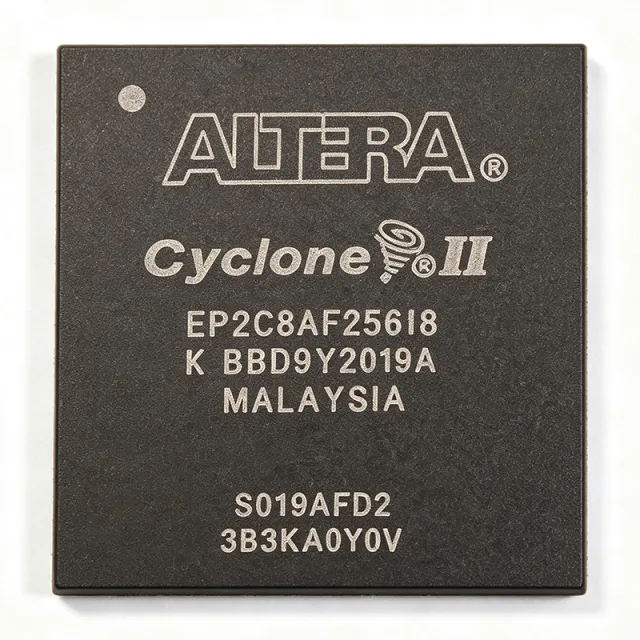
EP2C8AF256I8N - Cyclone II FPGA, 8256 LEs, 256-FBGA | Intel
MPN: EP2C8AF256I8N ✗ End of Life| Qty | Unit Price | Extended |
|---|---|---|
| 1 | $36.5 | $36.50 |
| 10 | $33.2 | $332.00 |
| 100 | $28.95 | $2,895.00 |
| 500 | $24.8 | $12,400.00 |
| 1,000 | $21.4 | $21,400.00 |
EP2C8AF256I8N Overview
What is an FPGA? A Field Programmable Gate Array is a programmable logic device that lets engineers implement arbitrary digital circuits after PCB fabrication, in contrast to an ASIC (Application-Specific Integrated Circuit) whose function is fixed at the foundry. FPGAs sit in the broader taxonomy of programmable logic devices (PLDs) > FPGAs > SRAM-based FPGAs > low-cost FPGAs, alongside SPLDs and CPLDs. Cyclone II occupies the entry-level/low-density node of this hierarchy, optimized for cost-per-logic-element rather than raw performance.
Key features include 36 embedded 18x18 multipliers (typical), up to 4 PLLs for clock management, support for external memory interfaces including DDR/DDR2/QDRII SRAM, and configuration via passive serial, active serial, or JTAG. The 1.2 V core supply with separate VCCIO banks (1.5 V / 1.8 V / 2.5 V / 3.3 V) allows mixed-voltage I/O without level shifters, which is a major advantage over older FPGAs with fixed I/O standards.
The Cyclone II architecture combines a 2-D row/column interconnect with embedded multiplier blocks and M4K RAM blocks (4 Kbit each, true dual-port), enabling efficient DSP and buffer implementations. 90 nm process technology balances leakage and performance for the target industrial and consumer segments.
Typical applications include industrial motor control, video processing bridges, low-cost PCIe endpoints, protocol bridging (UART/SPI/I2C aggregation), and LED display controllers. Designers choose Cyclone II when unit cost matters more than absolute logic density or transceiver speed.
Design consideration: PCB layout for a 256-ball FBGA demands 4 to 6 layer stackups with matched-impedance routing for clock and high-speed I/O. The I suffix in the part number denotes the industrial temperature range, which is the appropriate selection for non-automotive applications operating between -40C and +100C.
This page synthesizes distributor pricing, drop-in same-package alternatives, and practical design notes that go beyond the manufacturer datasheet to support rapid BOM decisions.
Drop-in alternatives for EP2C8AF256I8N — same package, pin-to-pin compatible. Different-package parts requiring PCB rework are excluded.
Variants in this series
Same-series models that are drop-in compatible with EP2C8AF256I8N (same form factor and footprint) — differing in Package, RoHS Status, Process Technology, Speed Grade, Operating Temperature.
Quick Comparison Tool — Select alternative parts for side-by-side comparison:
EP2C8F256I8N
✓ In Stock
$21.95 / Unit
View Datasheet →EP2C8AF256A7N
✓ In Stock
$41.5 / Unit
View Datasheet →EP2C8F256C8
✓ In Stock
$28.4 / Unit
View Datasheet →EP2C8F256C7
✓ In Stock
$18.2 / Unit
View Datasheet →EP2C5AF256I8N
✓ In Stock
$16.1 / Unit
View Datasheet →EP2C8AF256C7N
📋 Reference alternative (not in catalog)
EP2C8AF256I8N Maximum Ratings & Electrical Characteristics
| Family | Cyclone II |
| Logic Elements (LE) | 8,256 |
| Embedded Memory Bits | 165,888 bits (162 Kbit RAM) |
| Embedded Multipliers (18x18) | 36 |
| Maximum User I/O Pins | 182 |
| PLLs | 4 |
| Global Clocks | 16 |
| Configuration Elements | Embedded SRAM, JTAG, AS, PS |
| Core Voltage (VCCINT) | 1.2 V |
| I/O Voltage (VCCIO) | 1.5 V / 1.8 V / 2.5 V / 3.3 V (bank-selectable) |
| Process Technology | 90 nm CMOS, SRAM-based |
| Package | 256-ball FBGA (FineLine BGA) |
| Operating Temperature | -40C to +100C (Industrial, I suffix) |
| Mounting Type | Surface Mount (BGA) |
| RoHS Status | Lead-free (per Altera ordering code suffix) |
| Speed Grade | 8 |
| Status Suffix | N (lead-free, Pb-free) |
EP2C8AF256I8N Pin Configuration
| Pin A1 | I/O — User I/O, Bank 1 |
| Pin A2 | I/O — User I/O, Bank 1 |
| Pin A3 | I/O — User I/O, Bank 1 |
| Pin A4 | VCCIO1 — I/O supply Bank 1 |
| Pin B1 | I/O — User I/O, Bank 1 |
| Pin B2 | GND — Ground |
| Pin B3 | I/O — User I/O, Bank 1 |
| Pin B4 | I/O — User I/O, Bank 1 |
| Pin C1 | I/O — User I/O, Bank 2 |
| Pin C2 | I/O — User I/O, Bank 2 |
| Pin C3 | VCCIO2 — I/O supply Bank 2 |
| Pin C4 | I/O — User I/O, Bank 2 |
| Pin D1 | GND — Ground |
| Pin D2 | I/O — User I/O, Bank 2 |
| Pin D3 | I/O — User I/O, Bank 2 |
| Pin D4 | I/O — User I/O, Bank 2 |
| Pin E1 | I/O — User I/O, Bank 3 |
| Pin E2 | VCCIO3 — I/O supply Bank 3 |
| Pin E3 | I/O — User I/O, Bank 3 |
| Pin E4 | GND — Ground |
| Pin F1 | I/O — User I/O, Bank 4 |
| Pin F2 | I/O — User I/O, Bank 4 |
| Pin F3 | I/O — User I/O, Bank 4 |
| Pin F4 | VCCIO4 — I/O supply Bank 4 |
| Pin G1 | VCCINT — Core voltage 1.2 V |
| Pin G2 | I/O — User I/O, Bank 5 |
| Pin G3 | I/O — User I/O, Bank 5 |
| Pin G4 | GND — Ground |
| Pin H1 | I/O — User I/O, Bank 5 |
| Pin H2 | GND — Ground |
| Pin H3 | I/O — User I/O, Bank 5 |
| Pin H4 | VCCINT — Core voltage 1.2 V |
| Pin J1 | I/O — User I/O, Bank 6 |
| Pin J2 | VCCIO6 — I/O supply Bank 6 |
| Pin J3 | I/O — User I/O, Bank 6 |
| Pin J4 | I/O — User I/O, Bank 6 |
| Pin K1 | I/O — User I/O, Bank 6 |
| Pin K2 | I/O — User I/O, Bank 6 |
| Pin K3 | GND — Ground |
| Pin K4 | I/O — User I/O, Bank 6 |
| Pin L1 | VCCIO7 — I/O supply Bank 7 |
| Pin L2 | I/O — User I/O, Bank 7 |
| Pin L3 | I/O — User I/O, Bank 7 |
| Pin L4 | I/O — User I/O, Bank 7 |
| Pin M1 | GND — Ground |
| Pin M2 | I/O — User I/O, Bank 8 |
| Pin M3 | I/O — User I/O, Bank 8 |
| Pin M4 | VCCIO8 — I/O supply Bank 8 |
| Pin N1 | I/O — User I/O, Bank 8 |
| Pin N2 | I/O — User I/O, Bank 8 |
| Pin N3 | I/O — User I/O, Bank 8 |
| Pin N4 | GND — Ground |
| Pin P1 | TDI — JTAG Test Data In |
| Pin P2 | TMS — JTAG Test Mode Select |
| Pin P3 | TCK — JTAG Test Clock |
| Pin P4 | TDO — JTAG Test Data Out |
| Pin R1 | nCE — Chip Enable (active low) |
| Pin R2 | nCONFIG — Configuration Reset (active low) |
| Pin R3 | nSTATUS — Configuration Status (active low) |
| Pin R4 | CONF_DONE — Configuration Done (open-drain) |
| Pin T1 | CLK0 — Dedicated clock input 0 |
| Pin T2 | CLK1 — Dedicated clock input 1 |
| Pin T3 | DCLK — Configuration clock input |
| Pin T4 | MSEL0 — Configuration mode select |
Typical Applications
EP2C8AF256I8N is suitable for 6 applications: Industrial Motor Control, Video Processing Bridge, Low-Cost PCIe Endpoint, Protocol Bridging and Aggregation, LED Display Controller, Test and Measurement Front-End.
Industrial Motor Control
The EP2C8AF256I8N fits industrial motor control applications because its 8,256 logic elements and 36 embedded 18x18 multipliers can execute field-oriented control (FOC) and space-vector PWM algorithms in parallel hardware, while 182 user I/O pins handle quadrature encoder inputs, PWM outputs, and resolver feedback simultaneously. Industrial temperature grade (-40C to +100C) suits factory-floor and outdoor installations. Compared with a microcontroller-only solution, the FPGA offloads time-critical control loops, freeing the MCU for communication and supervisory tasks. Designers typically pair the EP2C8 with a Cortex-M4 MCU and gate drivers in a 3-phase inverter reference design.
Recommended
Video Processing Bridge
The EP2C8AF256I8N's 165,888 bits of embedded RAM and DDR/DDR2 memory controller support make it suitable for video format bridges between cameras, displays, and SoCs. Engineers use the 36 hardware multipliers to perform color-space conversion (YUV to RGB, BT.601 to BT.709) and scaling in real time at 60 Hz without overloading the host processor. The 256-FBGA package integrates cleanly onto 4-layer PCBs with controlled-impedance routing. Compared with discrete ASSP bridges, the Cyclone II offers flexible I/O voltage banks (1.5/1.8/2.5/3.3 V) for direct connection to legacy and modern image sensors.
Recommended
Low-Cost PCIe Endpoint
The EP2C8AF256I8N supports a PCIe x1 soft IP core with external PHY, making it suitable for low-cost endpoint cards in industrial PCs and instrumentation. Its 182 user I/O pins accommodate PCIe lane signals plus auxiliary GPIO for board-level control. The 4 PLLs generate the 100 MHz reference clock with fine granularity, while embedded RAM serves as PCIe transmit/receive FIFO buffers. Source: Altera Cyclone II PCIe x1 user guide. For higher lane counts (x4), designers typically migrate to Cyclone IV GX or Cyclone V GX families.
Recommended
Protocol Bridging and Aggregation
The EP2C8AF256I8N excels at protocol bridging where multiple UART/SPI/I2C/CAN ports must be aggregated into a single high-speed uplink (PCIe, USB 3.0, or gigabit Ethernet). Its hardware parallelism handles dozens of simultaneous low-speed channels without CPU intervention, while the 165 Kbits of block RAM buffer packets. Industrial temperature grade suits factory automation gateways. Compared with dedicated protocol switch ICs, the FPGA allows custom frame formats and proprietary protocols that no ASSP supports.
Recommended
LED Display Controller
The EP2C8AF256I8N drives large LED display walls in indoor commercial signage and stage lighting controllers. Its 36 hardware multipliers enable per-pixel brightness correction (gamma + color calibration) in real time, while 182 I/O pins handle HUB75-style row/column multiplex to hundreds of scan lines. Compared with dedicated LED driver ASSPs, the Cyclone II supports arbitrary resolution, refresh rates, and HDR pixel formats without firmware limitations. Designers typically pair it with MBI5024 or TLC5941 constant-current sink drivers.
Recommended
Test and Measurement Front-End
The EP2C8AF256I8N's 4 PLLs and 16 global clock networks make it suitable for test instrumentation front-ends (logic analyzers, protocol analyzers, and high-speed data acquisition). Its 36 embedded multipliers implement digital decimation filters and FFT pre-processing before offloading to a host PC over PCIe or USB. The 256-FBGA package supports dense BGA probe access for JTAG-driven boundary-scan. Industrial temperature grade allows bench and field-portable instruments operating between -40C and +100C. Source: Altera AN 486 reference design.
Recommended
Recommended Products Summary
Engineering reference data for EP2C8AF256I8N — comparison, design guidance, and compliance information.
Selection Guide
Comparison with Alternatives
| Parameter | This Product | EP2C8F256I8N | EP2C8AF256A7N | EP2C8AF256C7N | EP2C8F256C7 | EP2C5AF256I8N |
|---|---|---|---|---|---|---|
| Brand | Intel | Intel | Intel | Intel | Intel | Intel |
| Package | 256-FBGA (AF) | 256-FBGA (F) | 256-FBGA (AF) | 256-FBGA (AF) | 256-FBGA (F) | 256-FBGA (AF) |
| Logic Elements | 8,256 | 8,256 | 8,256 | 8,256 | 8,256 | 4,608 |
| Temperature Grade | Industrial (-40C to +100C) | Industrial (-40C to +100C) | Automotive (-40C to +125C) | Commercial (0C to +85C) | Commercial (0C to +85C) | Industrial (-40C to +100C) |
| Speed Grade | 8 | 8 | 7 | 7 | 7 | 8 |
| Embedded RAM | 165,888 bits | 165,888 bits | 165,888 bits | 165,888 bits | 165,888 bits | 119,808 bits |
| 18x18 Multipliers | 36 | 36 | 36 | 36 | 36 | 23 |
| PLLs | 4 | 4 | 4 | 4 | 4 | 2 |
| User I/O Max | 182 | 182 | 182 | 182 | 182 | 158 |
Key Differentiators
- Industrial temperature grade with speed grade 8 (vs EP2C8AF256C7N)
- 8,256 LEs with 36 multipliers in same 256-FBGA (vs EP2C5AF256I8N)
- AF package with lead-free fine-pitch BGA designation (vs EP2C8F256I8N)
Design Notes
Estimated: EP2C8AF256I8N core current at 1.2 V is approximately 0.5-1.2 A depending on logic utilization and clock rate; I/O current scales with switching frequency, output loading, and bank voltage. Per the Cyclone II power calculator, a typical 70% utilization design at 100 MHz consumes about 1.5 W. Use a 1.2 V LDO or buck regulator with at least 2 A headroom and place decoupling capacitors (0.1 uF and 10 uF) within 5 mm of every VCCINT/VCCIO pin.
The 256-ball FBGA package has a 1.0 mm ball pitch, requiring a 4- or 6-layer PCB with 0.4-0.5 mm via-in-pad or microvia escape for the inner row balls. Follow Intel's Cyclone II board design guidelines for BGA breakout, including matched-impedance routing for CLK/DDR signals (typically 50 ohm single-ended, 100 ohm differential). Do not route signals under the BGA if escape routing forces the trace through the inner ball rows.
Do not leave MSEL pins floating; tie them to VCCINT or GND per the desired configuration mode (AS, PS, JTAG). The nCONFIG pin requires an external 10 kohm pull-up to VCCIO. JTAG chain integrity requires TCK pulled low through 1 kohm and TMS pulled high through 1 kohm when unused. Configuration failure with CONF_DONE low after power-up typically indicates a corrupted bitstream or wrong MSEL settings - verify with the Quartus programmer.
Place the configuration device (EPCS4/EPCS16) within 50 mm of the FPGA to avoid signal integrity issues on the AS configuration interface. Keep DCLK and DATA0 traces short and matched (<25 mm). Series-terminate DCLK with 33 ohm if the trace exceeds 25 mm. All JTAG signals (TDI, TDO, TMS, TCK) should be routed on a single layer with a continuous ground reference and 10 kohm pull-up on TCK/TMS to VCCIO.
Compliance Information
Lead-free per 'N' suffix in MPN. RoHS compliance per Altera/Intel product page. Not AEC-Q100 qualified; for automotive designs use EP2C8AF256A7N (A-grade).


