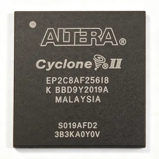
EP1K50FC256-1N - ACEX-1K 50K Gates 250MHz FPGA | Intel / Altera
MPN: EP1K50FC256-1N ✗ End of Life| Qty | Unit Price | Extended |
|---|---|---|
| 1 | $35.5 | $35.50 |
| 10 | $28.4 | $284.00 |
| 100 | $21.3 | $2,130.00 |
| 250 | $17.85 | $4,462.50 |
| 500 | $15.1 | $7,550.00 |
EP1K50FC256-1N Overview
An FPGA (Field-Programmable Gate Array) is a type of programmable logic device (PLD) that combines the high integration of a gate array with the field-programmability of a logic device. Within the broader taxonomy it sits under programmable logic -> PLD -> FPGA -> SRAM-based FPGA -> embedded-array FPGA. The ACEX-1K family specifically targets low-cost system-on-a-programmable-chip (SOPC) integration by combining a look-up-table (LUT) based logic fabric with on-chip dual-port RAM and embedded megafunction blocks, allowing designers to integrate glue logic, FIFOs, state machines, DSP datapaths, and bus interfaces in a single device.
Key features include 199,000 maximum system gates, 186 user I/O pins, support for multiple I/O standards including LVTTL, LVCMOS, PCI, and GTL+, dual-port embedded array blocks (EABs) usable as RAM/ROM or as megafunction hosts, and a typical operating current of 5 mA. The device is fabricated on a 0.22 um CMOS process and is powered from a single 2.5 V core supply (2.375 V to 2.625 V), with separate VCCIO banks for I/O standard compatibility.
Architecturally, the EP1K50FC256-1N combines 2,880 logic elements organized as 360 LABs (each LAB containing 8 LEs), interconnected by a FastTrack continuous routing architecture. The embedded array blocks (EABs) provide true dual-port RAM with synchronous operation and parity options, and the device supports Altera's Quartus (and legacy MAX+PLUS II) development flows. The maximum internal toggle frequency is specified at 250 MHz in the commercial -1 speed grade.
Typical applications include telecommunications line cards, industrial glue-logic and protocol bridging, low-volume ASIC replacement, PCI bridge and interface logic, motor-control state machines, and embedded control boards in factory automation and instrumentation.
When designing with this part, ensure the Quartus II (or MAX+PLUS II) toolchain is used for synthesis, place-and-route, and timing analysis. The 2.5 V core rail must be decoupled with a 0.1 uF ceramic capacitor placed within 5 mm of each VCC pin, and the JTAG pins (TCK/TMS/TDI/TDO and TRST) must be pulled or terminated according to the IEEE 1149.1 boundary-scan specification used by the device.
This page synthesizes distributor stock and pricing, drop-in alternative MPNs (same 256-FBGA package, same family), and practical design notes not collected together in the Altera datasheet itself, helping procurement and FPGA engineers evaluate the EP1K50FC256-1N at a glance.
Drop-in alternatives for EP1K50FC256-1N — same package, pin-to-pin compatible. Different-package parts requiring PCB rework are excluded.
Variants in this series
Same-series models that are drop-in compatible with EP1K50FC256-1N (same form factor and footprint) — differing in Process Technology, Configuration Method, Family, Package, Speed Grade.
Quick Comparison Tool — Select alternative parts for side-by-side comparison:
EP1K50FC256-1
✅ Drop-In ⚠️ 参数待验证✓ In Stock
$18.95 / Unit
View Datasheet →EP1K50FC256-2N
✅ Drop-In✓ In Stock
$17.95 / Unit
View Datasheet →EP1K50FC256-3N
✅ Drop-In✓ In Stock
$84 / Unit
View Datasheet →EP1K50FI256-2N
✅ Drop-In✓ In Stock
$23.9 / Unit
View Datasheet →EP1K50FC256-1N Maximum Ratings & Electrical Characteristics
| Family | ACEX-1K |
| Series | ACEX-1K (2.5 V) |
| Maximum Logic Elements | 2,880 |
| Logic Array Blocks (LABs) | 360 |
| Typical Gates | 50,000 |
| Maximum System Gates | 199,000 |
| Embedded Memory (EAB) Bits | 40,960 bits |
| User I/O Pins | 186 |
| Core Supply Voltage | 2.5 V (2.375 V to 2.625 V) |
| Maximum Internal Frequency | 250 MHz |
| Process Technology | 0.22 um CMOS |
| Typical Operating Current | 5 mA |
| Speed Grade | -1 (commercial) |
| Operating Temperature | 0 C to 70 C (commercial) |
| Package | 256-ball FBGA (FineLine BGA) |
| Mounting Type | Surface Mount |
| Lead Status | Lead-free (-N suffix) |
| RoHS Status | Compliant |
| Programmable I/O Standards | LVTTL, LVCMOS, PCI, GTL+ |
| Configuration Method | SRAM-based, JTAG (IEEE 1149.1) |
EP1K50FC256-1N 256-ball fbga (fineline bga) Pin Configuration Guide
Pin configuration for EP1K50FC256-1N (256-ball fbga (fineline bga) package). This digital IC includes GPIO, communication interfaces (UART, SPI, I2C), and power pins. Refer to the manufacturer datasheet for alternate pin functions and configuration options. Essential for embedded system design and PCB layout.

No detailed pinout data available for EP1K50FC256-1N.
Refer to the datasheet for full pin configuration.
Typical Applications
EP1K50FC256-1N is suitable for 6 applications: Telecommunications Line Card Glue Logic, PCI Bridge and Interface Logic, Industrial Glue-Logic and Protocol Bridging, Low-Volume ASIC Replacement, Motor-Control State Machines and PWM Generators, Test and Measurement Front-End Logic.
Telecommunications Line Card Glue Logic
The EP1K50FC256-1N fits telecommunications line-card glue-logic with 2,880 logic elements and 40,960 bits of dual-port RAM available to implement custom bus bridges, protocol adapters, and FIFO buffers between TDM backplanes and network processors. Its 186 user I/Os accommodate multi-standard bus fanout and the 250 MHz internal frequency supports 155 Mbps telecom interfaces. Placed as a coprocessor next to a network ASIC, it reduces BOM count compared to several discrete CPLDs and runs from a single 2.5 V rail that is already present on most telecom line cards.
Recommended
PCI Bridge and Interface Logic
The EP1K50FC256-1N is well-suited to PCI bridge, target, and custom-IO applications because it supports the 3.3 V / 5 V PCI signaling standard via its programmable I/O banks. With 2,880 logic elements and 186 I/Os, designers can implement a 32-bit/33 MHz PCI target plus register windows in one device. The 256-FBGA package exposes enough balls to fan out 32 data lines plus control, and Quartus II provides pre-built PCI megafunctions that map cleanly onto the device.
Recommended
Industrial Glue-Logic and Protocol Bridging
The EP1K50FC256-1N handles industrial glue-logic and protocol-bridging tasks such as SPI-to-parallel, I2C-to-Local-Bus, and UART-to-IO-link conversion in factory-automation boards. Its 0 C to 70 C commercial range is fine for control-cabinet equipment; for harsher -40 C to +85 C environments the EP1K50FI256-2N (industrial grade, same 256-FBGA package) is a pin-compatible substitute. The 40,960 bits of dual-port EAB memory can be configured as FIFOs to absorb bursts between mismatched clock domains common in factory protocols.
Recommended
Low-Volume ASIC Replacement
The EP1K50FC256-1N replaces low-volume gate-array or standard-cell ASICs at a fraction of NRE cost, making it ideal for products shipping in the hundreds to low thousands of units per year. With 199,000 max system gates and 186 I/Os, designers can integrate glue logic, register sets, FIFOs, and bus interfaces that previously required a custom ASIC. The mature Quartus II flow shortens development time and the SRAM-based configuration supports field updates via JTAG.
Recommended
Motor-Control State Machines and PWM Generators
The EP1K50FC256-1N implements multi-axis motor-control state machines, PWM generators, and quadrature-encoder counters in industrial drives and CNC controllers. Its 250 MHz internal frequency and 186 I/Os support several encoder channels and PWM outputs simultaneously, while the embedded dual-port RAM holds look-up tables for sinusoidal commutation profiles. When paired with external gate drivers and ADCs, this FPGA becomes the central timing engine for a complete digital motor controller.
Recommended
Test and Measurement Front-End Logic
The EP1K50FC256-1N is a strong fit for test-and-measurement front-end logic where it sequences measurement cycles, formats data for downstream processors, and implements custom trigger logic. Its 40,960 bits of dual-port RAM build acquisition FIFOs between ADCs and USB/Ethernet controllers, and the 250 MHz internal clock supports real-time trigger decisions at sub-microsecond latency. Designers leverage Quartus II megafunctions to instantiate UARTs, I2C, and SPI cores alongside the measurement-specific state machine.
Recommended
Recommended Products Summary
Engineering reference data for EP1K50FC256-1N — comparison, design guidance, and compliance information.
Selection Guide
Comparison with Alternatives
| Parameter | This Product | EP1K50FC256-1 | EP1K50FC256-2N | EP1K50FC256-3N | EP1K50FI256-2N |
|---|---|---|---|---|---|
| Brand | Intel (formerly Altera) | Intel (formerly Altera) | Intel (formerly Altera) | Intel (formerly Altera) | Intel (formerly Altera) |
| Package | 256-FBGA (FC) | 256-FBGA (FC) - same | 256-FBGA (FC) - same | 256-FBGA (FC) - same | 256-FBGA (FI) - same BGA ball count, pinout to verify |
| Speed Grade | -1 (commercial, slowest) | -1 (leaded) | -2 (faster) | -3 (fastest commercial) | -2 industrial |
| Max Internal Frequency | 250 MHz | 250 MHz | ~350 MHz | ~400 MHz | ~350 MHz |
| Logic Elements | 2,880 | 2,880 | 2,880 | 2,880 | 2,880 |
| Embedded RAM | 40,960 bits | 40,960 bits | 40,960 bits | 40,960 bits | 40,960 bits |
| User I/O | 186 | 186 | 186 | 186 | 186 |
| Operating Temperature | 0 C to 70 C (commercial) | 0 C to 70 C (commercial) | 0 C to 70 C (commercial) | 0 C to 70 C (commercial) | -40 C to +85 C (industrial) |
| Lead Status | Lead-free (-N) | Leaded (non-N) | Lead-free (-N) | Lead-free (-N) | Lead-free (-N) |
| Lifecycle Status | Obsolete (last-time-buy closed) | Obsolete | Obsolete | Obsolete | Obsolete |
Key Differentiators
- Lead-free (RoHS-compliant) -1 speed grade variant (vs EP1K50FC256-1)
- Commercial temperature range 0 C to 70 C matches typical office/control-cabinet deployments (vs EP1K50FI256-2N)
- Slowest speed grade (-1) gives the largest timing margin for simple glue logic (vs EP1K50FC256-2N)
- Mature Quartus II / MAX+PLUS II toolchain support (vs EP1K100FC256-1N)
Design Notes
Estimated: at VCC = 2.5 V and I_CC(core) = 5 mA typical plus I/O switching current, a single 0.1 uF ceramic decoupling capacitor per VCC ball (256 balls) keeps the high-frequency supply ripple within the device's tolerance. Place each capacitor within 5 mm of its corresponding VCC ball and add a few bulk 10 uF to 22 uF tantalum or ceramic capacitors around the BGA periphery. Power-on ramp should be monotonic between 1 ms and 100 ms per the ACEX-1K configuration guide.
The 256-FBGA has a 1.0 mm or 1.27 mm ball pitch (verify exact dimension against the device-specific datasheet drawing). Use a minimum 4-layer PCB with continuous VCC and GND planes under the BGA. Escape traces on the top layer between BGA balls should be 0.1 mm (4 mil) line and 0.1 mm space; fan-out to inner layers via microvias if manufacturing supports it. X-ray or endoscopic inspection is recommended after reflow because BGA solder joints are not visually inspectable.
ACEX-1K I/O pins support LVTTL, LVCMOS, PCI, and GTL+ standards. For PCI signaling, route 32-bit data buses with 50 ohm controlled impedance and length-match within +/- 8 mm. Because SRAM-based FPGAs drive I/O transitions synchronously across all pins, place series damping resistors on clock outputs that drive multiple loads to reduce simultaneous-switching noise (SSN) and supply bounce.
Common pitfalls: (1) ignoring the configuration mode pins (MSEL) and leaving them floating, which can leave the FPGA unconfigured or in the wrong mode after power-up; (2) failing to provide a JTAG chain connection (TCK/TMS/TDI/TDO/TRST) - this prevents in-system programming and boundary-scan test; (3) mixing commercial and industrial temperature parts on the same board lot, which leads to field failures at the cold or hot extremes. Always mark the temperature grade on the BOM.
Estimated: at typical operating current of 5 mA core and 2.5 V supply, the EP1K50FC256-1N dissipates approximately 12.5 mW core plus I/O switching power. Forced-air cooling is generally not required at low toggle rates, but designs switching many I/Os at 250 MHz should include a thermal copper pour under the BGA to spread heat. Refer to the ACEX-1K datasheet thermal resistance (theta_JA) section before derating for sealed enclosures.
Compliance Information
Lead-free (-N suffix) per the Altera/Intel product marking. RoHS-compliant per distributor listings. ACEX-1K is a commercial-grade FPGA family, so AEC-Q100 automotive qualification is not applicable.