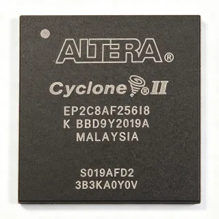
EPF10K100EFC256-3 - 100K Gates FLEX 10KE FPGA, 256-BGA | Intel
MPN: EPF10K100EFC256-3 ✗ End of Life| Qty | Unit Price | Extended |
|---|---|---|
| 1 | $38.5 | $38.50 |
| 10 | $34.2 | $342.00 |
| 100 | $29.85 | $2,985.00 |
| 500 | $26.4 | $13,200.00 |
| 1,000 | $23.1 | $23,100.00 |
EPF10K100EFC256-3 Overview
What is an FPGA? A Field Programmable Gate Array is a reconfigurable semiconductor device built from an array of programmable logic blocks, interconnect, and I/O cells. FPGAs sit between fixed-function ASICs and software-programmable processors: they offer hardware-level parallelism and timing precision like an ASIC, but can be reconfigured in the field. The FLEX 10KE family, introduced by Altera (now Intel), was the industry's first embedded PLD family to combine a logic array with embedded array blocks (EABs) for on-chip memory, marking the industry's first System-on-a-Programmable-Chip (SOPC) integration.
Key features of the EPF10K100EFC256-3 include 191 maximum user I/Os (DigiKey listing) / 274 pins per alternate datasheet listing, built-in IEEE 1149.1-1990 JTAG boundary-scan test (BST) circuitry compliant with PCI Local Bus Specification Revision 2.2 at 33 MHz or 66 MHz for 3.3-V operation, and a 0.22-micron CMOS process technology enabling up to 200 MHz internal operation. The device uses CMOS logic at a 2.5V core and supports multi-voltage I/O standards including LVTTL, LVCMOS, PCI, and SSTL.
Technically, the FLEX 10KE architecture organizes logic into Logic Array Blocks (LABs) - the device contains 624 LABs - each containing 8 logic elements (LEs) with a 4-input look-up table. Embedded Array Blocks (EABs) deliver up to 2,048 bits of dual-port RAM per block, configurable as RAM, ROM, or product-term logic. The continuous FastTrack interconnect routes signals across rows and columns with predictable delay, enabling timing closure across complex designs.
Typical applications include PCI bus interface cards, telecommunications glue logic, industrial control adapters, prototyping for ASIC emulation, and high-speed data acquisition pre-processing. The -3 speed grade and 191 user I/Os make this device suitable for interface bridging and protocol conversion where deterministic timing is required.
When designing with this device, ensure JTAG chain integrity by including TMS, TCK, TDI, TDO, and TRST pull-up/pull-down resistors per IEEE 1149.1 conventions. For PCI applications at 66 MHz, restrict I/O placement to PCI-compliant banks and maintain reference-plane continuity under the BGA.
This page synthesizes distributor pricing, drop-in alternatives, and practical design notes not found in the manufacturer datasheet.
Drop-in alternatives for EPF10K100EFC256-3 — same package, pin-to-pin compatible. Different-package parts requiring PCB rework are excluded.
Variants in this series
Same-series models that are drop-in compatible with EPF10K100EFC256-3 (same form factor and footprint) — differing in Package, Process Technology, Operating Temperature, Speed Grade, Total RAM Bits.
Quick Comparison Tool — Select alternative parts for side-by-side comparison:
EPF10K100EFC256-2
✅ Drop-In ⚠️ 参数待验证✓ In Stock
$165 / Unit
View Datasheet →EPF10K100EFC256-2X
✅ Drop-In ⚠️ 参数待验证✓ In Stock
$30.5 / Unit
View Datasheet →EPF10K100EFC256-1
✅ Drop-In ⚠️ 参数待验证📋 Reference alternative (not in catalog)
EPF10K100BFC256-3
✅ Drop-In ⚠️ 参数待验证✓ In Stock
$58.2 / Unit
View Datasheet →EPF10K100BFC256-2
✅ Drop-In ⚠️ 参数待验证✓ In Stock
$65 / Unit
View Datasheet →EPF10K100EFC256-3 Maximum Ratings & Electrical Characteristics
| Family | FLEX 10KE |
| Logic Elements | 4,992 |
| System Gates | 100,000 (typical) |
| Embedded RAM Bits | 49,152 bits |
| Maximum User I/Os | 191 |
| Logic Array Blocks (LABs) | 624 |
| Maximum Internal Frequency | 200 MHz |
| Propagation Delay | 0.6 ns |
| Process Technology | 0.22 micron CMOS |
| Core Supply Voltage | 2.5 V |
| I/O Supply Voltage | 3.3 V |
| Logic Family | CMOS |
| Package | 256-ball FBGA (FineLine BGA) |
| Operating Temperature | 0C to +70C (commercial) |
| Speed Grade | -3 (faster) |
| JTAG Support | IEEE 1149.1-1990 compliant |
| PCI Compliance | PCI Local Bus Specification Rev 2.2 at 33/66 MHz |
EPF10K100EFC256-3 256-ball fbga (fineline bga) Pin Configuration Guide
Pin configuration for EPF10K100EFC256-3 (256-ball fbga (fineline bga) package). This digital IC includes GPIO, communication interfaces (UART, SPI, I2C), and power pins. Refer to the manufacturer datasheet for alternate pin functions and configuration options. Essential for embedded system design and PCB layout.

No detailed pinout data available for EPF10K100EFC256-3.
Refer to the datasheet for full pin configuration.
Typical Applications
EPF10K100EFC256-3 is suitable for 6 applications: PCI Bus Interface Cards, Industrial Control Glue Logic, ASIC Prototyping and Emulation, Telecommunications Protocol Bridges, High-Speed Data Acquisition Pre-Processing, Legacy Board Repair and Sustainment.
PCI Bus Interface Cards
The EPF10K100EFC256-3 is well-suited for PCI Local Bus Specification Revision 2.2 interface designs at 33 MHz or 66 MHz with 3.3V signaling. Its -3 speed grade provides the timing margin required for 66 MHz operation, while the 191 user I/Os comfortably accommodate 32-bit PCI plus ancillary control and status signals. The built-in IEEE 1149.1-1990 JTAG boundary-scan test (BST) circuitry simplifies board-level compliance testing, and the 256-ball FineLine BGA package keeps board area small while maintaining signal-integrity for the 66 MHz edge rates. For designs that can run at 33 MHz, the EPF10K100EFC256-2 drops in at the same footprint.
Recommended
Industrial Control Glue Logic
In industrial control and factory-automation backplanes, the EPF10K100EFC256-3 is used as protocol-conversion glue logic between legacy parallel buses and modern serial interfaces. The 4,992 logic elements and 624 LABs provide enough capacity for full bus-state machines and FIFOs, while the 49,152 bits of embedded RAM (EAB blocks) implement small dual-port buffers without external memory. The 0C to +70C commercial operating range covers most cabinet environments. The 256-ball FineLine BGA footprint supports a 4-layer PCB stackup with continuous reference planes under the BGA - essential for noise immunity near motor drives.
Recommended
ASIC Prototyping and Emulation
Engineers prototyping an ASIC design often map RTL onto the EPF10K100EFC256-3 because its 100K system gates approximate a mid-complexity ASIC block, and its 200 MHz internal operation supports realistic pre-silicon verification. The FLEX 10KE family was specifically designed as an SOPC platform, allowing the same RTL that will be synthesized for an ASIC to be loaded into the FPGA for board-level testing. Designers using this part as an emulation target should keep I/O assignments within the 191 user I/Os exposed in the 256-ball FineLine BGA package and use the -3 speed grade to maximize timing closure confidence.
Recommended
Telecommunications Protocol Bridges
Telecom line cards use the EPF10K100EFC256-3 as a low-density bridge between backplane SERDES devices and backplane bus controllers, where its combination of 191 user I/Os and 4,992 logic elements fits typical protocol-conversion workloads. The device's LVTTL/LVCMOS/PCI I/O support means it can interface directly to common telecom ASICs without external level shifters. The -3 speed grade keeps latency low for time-sensitive telecom flows, and the 256-ball FineLine BGA's controlled-impedance escape routing simplifies signal-integrity analysis on the backplane side.
Recommended
High-Speed Data Acquisition Pre-Processing
Data-acquisition front ends use the EPF10K100EFC256-3 to pre-process high-speed sample streams before handing them to a downstream processor. Its 49,152 bits of EAB-based dual-port RAM can buffer a few milliseconds of samples, and the 4,992 logic elements are enough to implement FIR filters, decimation stages, or trigger logic. The 200 MHz internal frequency supports pre-processing at rates exceeding the 66 MHz PCI output bandwidth, and the 256-ball FineLine BGA package keeps the analog front end isolated from digital switching noise by allowing short, controlled-impedance traces between the ADC and the FPGA I/O bank.
Recommended
Legacy Board Repair and Sustainment
Because the EPF10K100EFC256-3 is marked obsolete by Intel, long-lifecycle programs in aerospace, defense, and industrial automation still purchase it for sustainment repairs of boards originally designed around this part. Drop-in alternatives in the same 256-ball FineLine BGA footprint - particularly the EPF10K100EFC256-2 and EPF10K100BFC256-3 - allow repair depots to substitute equivalent parts without PCB rework. The -3 speed grade remains the preferred choice for legacy 66 MHz PCI repairs because timing-closure margins match the original qualification baseline.
Recommended
Recommended Products Summary
Engineering reference data for EPF10K100EFC256-3 — comparison, design guidance, and compliance information.
Selection Guide
Comparison with Alternatives
| Parameter | This Product | EPF10K100EFC256-2 | EPF10K100EFC256-2X | EPF10K100EFC256-1 | EPF10K100BFC256-3 | EPF10K100BFC256-2 |
|---|---|---|---|---|---|---|
| Brand | Intel | Intel | Intel | Intel | Intel | Intel |
| Package | 256-ball FineLine BGA | 256-ball FineLine BGA | 256-ball FineLine BGA | 256-ball FineLine BGA | 256-ball FineLine BGA | 256-ball FineLine BGA |
| Family | FLEX 10KE | FLEX 10KE | FLEX 10KE | FLEX 10KE | FLEX 10KB | FLEX 10KB |
| Speed Grade | -3 | -2 | -2X | -1 | -3 | -2 |
| Logic Elements | 4,992 | 4,992 | 4,992 | 4,992 | 4,992 | 4,992 |
| Embedded RAM Bits | 49,152 | 49,152 | 49,152 | 49,152 | 0 (no EAB) | 0 (no EAB) |
| Core Voltage | 2.5 V | 2.5 V | 2.5 V | 2.5 V | 2.5 V | 2.5 V |
| Embedded Array Blocks (EAB) | Yes | Yes | Yes | Yes | No | No |
| Lifecycle Status | Obsolete | Obsolete | Obsolete | Obsolete | Obsolete | Obsolete |
Key Differentiators
- Fastest speed grade in the FLEX 10KE family (vs EPF10K100EFC256-2)
- Includes Embedded Array Blocks (EAB) for on-chip dual-port RAM (vs EPF10K100BFC256-3)
- Pin-compatible migration across the FLEX 10KE speed grade ladder (vs EPF10K100EFC256-2X)
Design Notes
The FLEX 10KE core runs from a 2.5V supply while I/O banks accept 3.3V. Decouple the core plane with one 10uF bulk plus one 0.1uF per power pin placed within 100 mil of each VCCINT ball. For 3.3V VCCIO, replicate the bulk/cap pattern on the I/O plane. Estimated: with 4,992 LEs switching at 200 MHz, expect ICCINT in the 200-500 mA range; ICCIO depends on I/O count and toggle rate, plan for at least 1A per bank.
The 256-ball FineLine BGA uses 1.0 mm pitch. Escape routing requires a 4-layer stackup with a continuous ground plane directly under the BGA to control return current. Use 8-mil microvias with via-in-pad if available; otherwise dog-bone fanout is acceptable but requires careful plane continuity. JTAG pins TMS, TCK, TDI, TDO, and TRST must each have a defined logic level per IEEE 1149.1 - pull TMS and TDI up through 10 kohm, pull TCK and TRST down through 10 kohm if no JTAG is connected.
For 66 MHz PCI operation, restrict I/O placement to the PCI-compliant banks and use the on-chip PCI clamp diodes by enabling the PCI I/O standard in the Quartus/MAX+PLUS II assignment editor. Maintain 50 ohm (single-ended) trace impedance to the connector. The -3 speed grade provides the timing margin required for 66 MHz; designs that drop to -2 must be re-verified with the worst-case timing model because the 66 MHz PCI eye shrinks.
Do not assume all 274 balls listed in some datasheet excerpts are user I/Os - the operative figure is 191 user I/Os as cited by DigiKey and Mouser for the EPF10K100EFC256-3. The part is marked obsolete by Intel, so new designs should target a current-generation device (Cyclone, MAX) or use the FLEX 10KE SameFrame pin-compatible migration to a 484-ball FineLine BGA for higher I/O. Do not confuse the FLEX 10KE (with EAB blocks) with the FLEX 10KB (no EAB blocks) - designs that rely on EAB-based dual-port RAM will not work on the FLEX 10KB family.
Place decoupling capacitors on the solder side directly beneath their respective BGA balls where possible, using short, wide traces to minimize loop inductance. Keep clock input pins away from high-toggle-rate I/O to reduce crosstalk; the FLEX 10KE's FastTrack interconnect is predictable but does not eliminate edge-to-edge coupling. For 3.3V PCI applications, route VCCIO as a star or wide plane to support the higher inrush current at insertion, and add a bulk capacitor at the PCI connector.
Compliance Information
RoHS, REACH, and halogen-free status were not explicitly listed in the provided web data; the part is marked obsolete by Intel. The part is commercial temperature grade (0C to +70C) and not AEC-Q100 qualified. PCI compliance per Local Bus Specification Revision 2.2 is documented in the manufacturer datasheet.