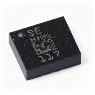
ESDALC6V1-5BTG - 5-Line ESD Protection TVS, 6.1V | STMicro
MPN: ESDALC6V1-5BTG ✓ Active| Qty | Unit Price | Extended |
|---|---|---|
| 1 | $0.12 | $0.12 |
| 10 | $0.09 | $0.90 |
| 100 | $0.06 | $6.00 |
| 500 | $0.045 | $22.50 |
| 1,000 | $0.035 | $35.00 |
ESDALC6V1-5BTG Overview
An ESD protection array (also called a TVS diode array or Transil array) is a class of transient voltage suppressor that clamps fast, high-energy voltage spikes on signal lines before they can damage sensitive downstream ICs. Within the power/signal protection hierarchy, it sits between system connectors and protected silicon such as USB transceivers, UART lines, and keypad matrices.
Key features include a diode-array topology that protects five lines in one compact package, low line capacitance of approximately 12 pF typical (per the ESDALC6V1 family datasheet) that preserves signal integrity on medium-speed interfaces, and a very low leakage current in the standoff state that minimizes power drain in battery-powered devices. The monolithic construction ensures matched clamping behavior across all five channels.
Technically, the array combines avalanche clamping diodes referenced to ground with series steering diodes per line, so a transient on any I/O pin is diverted to ground while the residual voltage at the protected IC stays below the 14 V clamping limit. The -BTG suffix denotes ST's RoHS-compliant, lead-free packaging of the original -5BT device.
Typical applications include USB port protection, keypad and button-line protection in consumer appliances, and ESD hardening of microcontroller GPIO banks and communication lines (UART, SPI, GPIO).
Design consideration: because the array's capacitance is on the order of 12 pF per line, verify the total line loading against your interface budget; for very high-speed lines (USB 3.x, MIPI), select a lower-capacitance ESD part instead.
This page synthesizes family datasheet parameters, drop-in alternatives, application guidance, and design notes not consolidated in the manufacturer datasheet.
Drop-in alternatives for ESDALC6V1-5BTG — same package, pin-to-pin compatible. Different-package parts requiring PCB rework are excluded.
Quick Comparison Tool — Select alternative parts for side-by-side comparison:
ESDALC6V1-5BT
✅ Drop-In ⚠️ 参数待验证📋 Reference alternative (not in catalog)
ESDALC6V1-5T6
✅ Drop-In📋 Reference alternative (not in catalog)
ESDALC6V1-5BTG Specifications
| Number of Protected Lines | 5 |
| Topology | Diode array (monolithic) |
| Reverse Standoff Voltage (VRWM) | 5 V |
| Breakdown Voltage (VBR) | 6.1 V (min) |
| Clamping Voltage (VCL) | 14 V max at IPP = 2.5 A (8/20 us) |
| Peak Pulse Current (IPP) | 2.5 A (8/20 us) |
| Input Capacitance | 12 pF (typical) |
| ESD Withstand | IEC 61000-4-2 level 4 (per family datasheet) |
| Package | SOT-23-6 |
| Mounting Type | Surface Mount |
| RoHS Status | Compliant (-G suffix indicates lead-free/RoHS packaging) |
| Brand / Manufacturer | STMicroelectronics |
ESDALC6V1-5BTG Pin Configuration
| Pin 1 | IO1 — Protected line 1 (steering diode input) |
| Pin 2 | GND — Ground / clamp reference |
| Pin 3 | IO2 — Protected line 2 |
| Pin 4 | IO3 — Protected line 3 |
| Pin 5 | IO4 — Protected line 4 |
| Pin 6 | IO5 — Protected line 5 |
Typical Applications
ESDALC6V1-5BTG is suitable for 6 applications: USB Port Protection, Keypad and Button Line Protection, Microcontroller GPIO Bank Protection, UART and Serial Communication Line Protection, Consumer Electronics Connector Hardening, Industrial I/O and Sensor Line Protection.
USB Port Protection
The ESDALC6V1-5BTG fits USB port protection because its 5V reverse standoff voltage matches the VBUS-referenced logic environment and its diode-array topology covers the D+, D-, and ID/CC lines plus auxiliary signals in one SOT-23-6 footprint. The 14V clamping voltage at 2.5A (8/20 us) keeps residual transient voltage below levels that endanger USB transceivers, while IEC 61000-4-2 level capability handles direct contact discharges at the connector. Placed as close to the USB receptacle as possible, the array diverts ESD strike energy to ground before it propagates down the data traces. The roughly 12 pF typical line capacitance is acceptable for Full-Speed and High-Speed USB 2.0, but designers targeting 480 Mbps should budget eye-mask margin for the added RC loading; for SuperSpeed pairs, a dedicated low-capacitance ESD part is preferable.
Recommended
Keypad and Button Line Protection
Human contact is the dominant ESD entry path for keypad matrices and button lines in appliances, meters, and consumer electronics. The ESDALC6V1-5BTG protects five such lines simultaneously in one SOT-23-6 package, replacing five discrete diodes and reducing placement cost and board area. Its 6.1V breakdown and 14V clamping at 2.5A safely absorb discharges from user fingers while the 5V standoff tolerates standard 3.3V and 5V GPIO rails without conducting in normal operation. Because keypad lines are low-speed, the approximately 12 pF typical capacitance has no functional penalty, making this array an ideal fit where integration matters more than ultra-low capacitance. Place the array at the point where the key matrix enters the PCB, with a short, low-inductance ground connection to the chassis or signal ground to maximize clamp effectiveness.
Recommended
Microcontroller GPIO Bank Protection
External connectors wired to microcontroller GPIO banks are classic ESD failure points: a single human-body discharge can punch through a pin's input protection and kill the MCU. The ESDALC6V1-5BTG shields five GPIO lines at once, with a 5V standoff that suits both 3.3V and 5V logic and a 14V clamp ceiling that keeps transients below the MCU's absolute maximum ratings. Its monolithic construction gives matched clamping across channels, avoiding the channel-to-channel variation seen when mixing discrete diodes. Signal-integrity impact is negligible on low-to-medium speed digital lines given the 12 pF typical capacitance. For best results, place the array within a few millimeters of the connector, route a solid ground plane under it, and keep the protected-side traces short so residual clamped energy cannot couple into neighboring high-impedance nodes.
Recommended
UART and Serial Communication Line Protection
UART, RS-232-adjacent, and other serial links that exit the enclosure via service connectors are exposed to ESD during maintenance and field use. The ESDALC6V1-5BTG protects TX, RX, RTS/CTS, and a control line in a single SOT-23-6 package, with the 6.1V breakdown and 14V clamp matching 5V-class transceiver inputs. Because UART data rates are low (typically under 1 Mbps), the approximately 12 pF per-line capacitance causes no edge degradation, so the array can be applied without signal-integrity analysis. IEC 61000-4-2 level transient capability at the connector satisfies most industrial and consumer robustness requirements when combined with a solid ground reference. Verify that the protected transceiver's absolute maximum pin voltage exceeds the 14V clamp figure; most 5V-tolerant UART transceivers meet this with margin.
Recommended
Consumer Electronics Connector Hardening
Consumer devices - set-top boxes, chargers, toys, white goods - expose multiple connectors to frequent human contact, and field-return analysis routinely identifies ESD-damaged port ICs as the top failure mode. The ESDALC6V1-5BTG offers a low-cost, five-line insurance policy: at roughly a few cents per protected line in volume (as of 2026-09-11), it hardens an entire connector with one SOT-23-6 placement. The RoHS-compliant -G packaging supports global environmental regulations, and the surface-mount format fits standard reflow assembly without special handling. Its 5V standoff, 6.1V breakdown, and 14V clamping cover the common 3.3V/5V signal ecosystem in these products. Designers should keep the array's ground return path short and wide; clamp performance degrades rapidly with added ground inductance at sub-nanosecond ESD rise times.
Recommended
Industrial I/O and Sensor Line Protection
Industrial panels route sensor and actuator signals to operator-accessible terminals, where cable handling and charged-operator discharge are routine. The ESDALC6V1-5BTG protects five such signal lines at the terminal block boundary, providing 14V clamping at 2.5A (8/20 us) so the PLC or sensor front-end sees only clamped residuals. The 5V standoff and 6.1V breakdown suit standard industrial logic levels, and the array's matched monolithic channels keep protection thresholds uniform across multi-line sensors such as encoders or proximity switches. Its SOT-23-6 footprint minimizes the protection-area penalty in dense I/O panels. Note that ESD arrays address fast, low-energy transients only; for surge events covered by IEC 61000-4-5 (e.g., long cable induction), pair the array with a higher-energy TVS such as an SMBJ series part and current-limiting series resistance.
Recommended
Recommended Products Summary
Engineering reference data for ESDALC6V1-5BTG — comparison, design guidance, and compliance information.
Selection Guide
Comparison with Alternatives
| Parameter | This Product | ESDALC6V1-5BT | ESDALC6V1-5T6 |
|---|---|---|---|
| Package | SOT-23-6 | SOT-23-6 - same | SOT-23-6 - same |
| Brand | STMicroelectronics | STMicroelectronics | STMicroelectronics |
| Protected Lines | 5 | 5 | 5 |
| Reverse Standoff Voltage | 5 V | 5 V | 5 V |
| Breakdown Voltage (min) | 6.1 V | 6.1 V | 6.1 V |
| Clamping Voltage | 14 V at 2.5 A (8/20 us) | 14 V at 2.5 A (8/20 us) | 14 V at 2.5 A (8/20 us) |
| Line Capacitance (typ) | 12 pF | 12 pF | 12 pF |
Key Differentiators
- Five protected lines in a single SOT-23-6 (vs ESD9B3.3ST5G)
- RoHS-compliant -G packaging (vs ESDALC6V1-5BT)
- Larger, easier-to-assemble package than SOT-666 variant (vs ESDALC6V1-5P6)
Design Notes
Place the ESDALC6V1-5BTG as close as possible to the ESD entry point (connector or terminal block), before any series resistors or protection circuitry. ESD transients have sub-nanosecond rise times, so every millimeter of trace before the array adds inductance that lets voltage build up on the protected line. Use a short, direct via to a solid ground plane for the GND pin (pin 2); a long ground return path is the most common reason a well-chosen ESD array fails in system-level IEC 61000-4-2 testing.
The array presents approximately 12 pF of typical capacitance per protected line. On low- and medium-speed interfaces (UART, GPIO, keypad) this is negligible, but on USB 2.0 High-Speed (480 Mbps) it contributes to the total channel loading and can affect the eye diagram margin. Estimated: a 12 pF load with typical 33 ohm source impedance yields a rise-time contribution on the order of 0.4 ns, which usually remains within USB 2.0 margins but should be simulated for borderline designs. For USB 3.x or MIPI lanes, select a dedicated sub-1 pF ESD device instead.
Do not exceed the 5V reverse standoff voltage on any I/O pin in normal operation - the steering diodes will begin to conduct and can be destroyed by sustained DC current. The array protects against fast transients only; it is not a surge suppressor for IEC 61000-4-5 class energy, so coordinate it with a higher-power TVS (e.g., SMBJ series) and series impedance on lines exposed to induced surges. Also confirm the protected IC's absolute maximum pin voltage exceeds the 14V clamp ceiling.
Compliance Information
RoHS compliance inferred from ST -G suffix nomenclature (lead-free/RoHS packaging). REACH, halogen-free, and conflict-minerals status not stated in verified data; confirm via ST product page or material declaration.