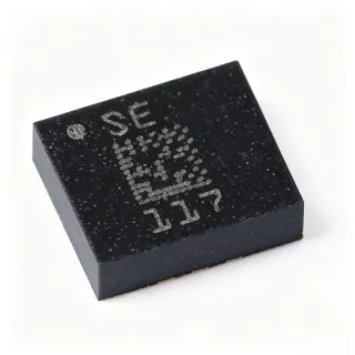
STM32F765VIH6 - 216MHz Cortex-M7 MCU 2MB Flash | ST
MPN: STM32F765VIH6 ✓ Active| Qty | Unit Price | Extended |
|---|---|---|
| 1 | $14.2 | $14.20 |
| 10 | $12.85 | $128.50 |
| 100 | $11.6 | $1,160.00 |
| 500 | $10.75 | $5,375.00 |
| 1,000 | $9.9 | $9,900.00 |
STM32F765VIH6 Overview
A microcontroller (MCU) is a single-chip computer that integrates a processor core, memory, and peripherals onto one die, serving as the computational heart of embedded systems. Within the system hierarchy, the STM32F765 belongs to the STM32F7 Series of high-performance MCUs, which sits above mainstream Cortex-M4 families and below multicore application processors, making it the workhorse choice for demanding real-time embedded control.
Key features include the Arm Cortex-M7 core with double-precision FPU and Armv7E-M DSP instructions, the adaptive real-time (Art) memory accelerator that achieves 0-wait-state execution from Flash at 216 MHz, and L1 instruction and data caches that maximize performance from external memory. Peripherals include SDRAM interface support, DFSDM (digital filter for sigma-delta modulators), multiple high-speed communication interfaces, and advanced analog blocks suitable for motor control and digital power.
Architecturally, the Art Accelerator and 16-Kbyte L1 instruction cache allow the Cortex-M7 to sustain its full 1082 CoreMark/MHz-class throughput even when fetching from on-chip Flash, a key differentiator from earlier Cortex-M families that required SRAM execution for peak performance. The double-precision FPU accelerates scientific and signal-processing math natively without software emulation.
Typical applications include industrial motor drives and digital power conversion (leveraging DFSDM and high-resolution timers), medical and test instrumentation requiring 216 MHz DSP throughput, and high-end consumer devices with graphical displays driven via SDRAM and LCD interfaces.
A key design consideration: the TFBGA package demands careful PCB design with controlled-impedance fanout, and the low core voltage is generated by an embedded regulator, so follow ST layout guidelines for VCAP capacitors and decoupling.
This page synthesizes distributor pricing, verified drop-in alternatives, design guidance, and application notes not consolidated in the manufacturer datasheet.
Drop-in alternatives for STM32F765VIH6 — same package, pin-to-pin compatible. Different-package parts requiring PCB rework are excluded.
Variants in this series
Same-series models that are drop-in compatible with STM32F765VIH6 (same form factor and footprint) — differing in L1 Cache.
Quick Comparison Tool — Select alternative parts for side-by-side comparison:
STM32F765IIH6
✅ Drop-In ⚠️ 参数待验证📋 Reference alternative (not in catalog)
STM32F767IIH6
✅ Drop-In ⚠️ 参数待验证📋 Reference alternative (not in catalog)
STM32F769IIH6
✅ Drop-In ⚠️ 参数待验证📋 Reference alternative (not in catalog)
STM32F750IIH6
✅ Drop-In ⚠️ 参数待验证📋 Reference alternative (not in catalog)
STM32F765VIH6 Maximum Ratings & Electrical Characteristics
| Core Processor | ARM Cortex-M7 32-bit RISC |
| Core Frequency | 216 MHz |
| Flash Memory | 2 MB (2M x 8) |
| Core Performance | 462 DMIPS |
| FPU | Yes (double-precision) |
| DSP Instructions | Yes |
| Memory Accelerator | Art Accelerator |
| L1 Cache | Yes (instruction + data) |
| SDRAM Interface | Yes |
| DFSDM | Yes (digital filter for sigma-delta modulators) |
| Supply Voltage | 3.3 V |
| Package | 100-TFBGA (8x8 mm) |
| Mounting Type | Surface Mount |
| Packaging | Tray |
| Product Status | Active |
STM32F765VIH6 100-tfbga (8x8 mm) Pin Configuration Guide
Pin configuration for STM32F765VIH6 (100-tfbga (8x8 mm) package). This digital IC includes GPIO, communication interfaces (UART, SPI, I2C), and power pins. Refer to the manufacturer datasheet for alternate pin functions and configuration options. Essential for embedded system design and PCB layout.

No detailed pinout data available for STM32F765VIH6.
Refer to the datasheet for full pin configuration.
Typical Applications
STM32F765VIH6 is suitable for 6 applications: Industrial Motor Drives and Digital Power, Human-Machine Interface and Graphics, Medical and Lab Instrumentation, Test and Measurement Equipment, Building Automation and IoT Gateways, Aerospace and High-Performance Embedded Control.
Industrial Motor Drives and Digital Power
The STM32F765VIH6 fits industrial motor control because its DFSDM interfaces directly with external sigma-delta modulators for high-resolution phase-current sensing, while the 216 MHz Cortex-M7 with double-precision FPU executes field-oriented control (FOC) loops with large timing margin. The DSP instruction set accelerates Park/Clarke transforms and PI controllers natively. In a typical servo drive, the MCU runs the current loop at 16-32 kHz with sensors sampled through DFSDM sinc filters, leaving headroom for position control and industrial communication stacks. Unlike lower-tier M4 MCUs, the FPU avoids fixed-point scaling work and the L1 caches sustain deterministic throughput from Flash via the Art Accelerator.
Recommended
Human-Machine Interface and Graphics
Although the F765 omits the LCD-TFT controller of the F767 sibling, its 216 MHz core, SDRAM interface, and 2 MB Flash make it capable of driving graphics via SPI/QSPI displays or serving as the HMI application processor in panels using external display controllers. The FMC SDRAM interface provides dedicated frame-buffer memory, and the Art Accelerator with L1 caches keeps UI rendering code executing at full speed from Flash. Typical implementations render to an SDRAM frame buffer and stream to a display bridge over high-speed SPI. The trade-off versus F767: no hardware TFT controller, so refresh is CPU-assisted, suiting simpler menus rather than full-video UIs.
Recommended
Medical and Lab Instrumentation
The STM32F765VIH6 suits medical and laboratory instrumentation where 462 DMIPS of DSP throughput processes signals from high-resolution converters. The DFSDM connects to external sigma-delta modulators used in precision weigh scales, biosignal amplifiers, and spectrum-analysis front ends, providing programmable sinc filtering in hardware. The double-precision FPU executes FFTs and calibration mathematics without fixed-point compromise, and 2 MB of Flash holds protocol stacks plus logging frameworks. In a patient-monitoring front end, for example, the MCU samples ECG channels through DFSDM at kilohertz rates, applies digital filtering, and streams results over USB or Ethernet-class connectivity with real-time guarantees.
Recommended
Test and Measurement Equipment
Bench instruments benefit from the STM32F765VIH6's combination of high core speed, DFSDM, and generous Flash for command parsers and DSP pipelines. At 216 MHz, the MCU can sustain waveform post-processing, trigger decision logic, and communication interfaces concurrently; the L1 caches hide Flash latency during compute bursts executed from cached SRAM regions. Its SDRAM interface buffers long capture records, while the FPU accelerates measurement algorithms such as RMS, THD, and windowed-FFT computations. Compared with running the same pipeline on a mainstream M4, the M7's superscalar-like dual-issue capability roughly doubles available DSP throughput at similar power.
Recommended
Building Automation and IoT Gateways
The STM32F765VIH6 serves as a gateway-class controller in building automation, aggregating multiple field buses while running protocol conversion and edge logic. Its 2 MB Flash accommodates concurrent stacks (for example Modbus plus IP-based protocols), the 216 MHz core handles TLS-class cryptographic workloads acceptably for an MCU, and the SDRAM interface adds working memory for packet buffers and data logging. Integrated high-speed peripherals reduce external component count compared with two-chip processor-plus-Bridge architectures. Designs typically pair the MCU with isolated transceivers on its UARTs and use its timers for pulse-based energy metering inputs, achieving single-chip gateway functionality with industrial-grade determinism.
Recommended
Aerospace and High-Performance Embedded Control
For demanding embedded control in UAVs, avionics support equipment, and rugged industrial systems, the STM32F765VIH6 provides 462 DMIPS in a compact 8x8 mm BGA, reducing board area versus larger SoM solutions. The Art Accelerator guarantees 0-wait-state Flash execution, important for flight-control loops where worst-case timing matters, and the double-precision FPU runs navigation and attitude-estimation math (quaternion kinematics, Kalman filters) natively. The SDRAM interface supports sensor data logging, while 2 MB Flash stores parameter tables and firmware with room for dual-bank OTA update schemes. Thermal design for the TFBGA package follows standard BGA array rules with ground-ball thermal vias.
Recommended
Recommended Products Summary
Engineering reference data for STM32F765VIH6 — comparison, design guidance, and compliance information.
Selection Guide
Comparison with Alternatives
| Parameter | This Product | STM32F765IIH6 | STM32F767IIH6 | STM32F769IIH6 | STM32F750IIH6 |
|---|---|---|---|---|---|
| Package | TFBGA-100 (8x8 mm) | TFBGA-100 (8x8 mm) - same | TFBGA-100 (8x8 mm) - same | TFBGA-100 (8x8 mm) - same | TFBGA-100 (8x8 mm) - same |
| Brand | STMicroelectronics | STMicroelectronics | STMicroelectronics | STMicroelectronics | STMicroelectronics |
| Core / Frequency | Cortex-M7 / 216 MHz | Cortex-M7 / 216 MHz | Cortex-M7 / 216 MHz | Cortex-M7 / 216 MHz | Cortex-M7 / 216 MHz |
| Flash Memory | 2 MB | 2 MB | 2 MB | 2 MB | 512 KB |
| Core Performance | 462 DMIPS | 462 DMIPS | 462 DMIPS | 462 DMIPS | 462 DMIPS |
| DFSDM | Yes | Yes | Yes | Yes | Yes |
| LCD-TFT / Chrom-ART Graphics | No | No | Yes | Yes | Yes |
| SDRAM Interface | Yes | Yes | Yes | Yes | Yes |
Key Differentiators
- Functionally identical same-silicon fallback (vs STM32F765IIH6)
- DFSDM-equipped control platform at lower cost than graphics variants (vs STM32F767IIH6)
- Largest on-chip Flash in the TFBGA100 family lineup (vs STM32F750IIH6)
Design Notes
The 100-TFBGA 0.8 mm ball pitch requires a careful fanout strategy. Use via-in-pad or dogbone fanouts on the outer two ball rows and plan inner-row escape routing on inner layers before starting placement. Provide a solid ground plane directly under the die and connect the ground balls with multiple vias for both return-current integrity and heat spreading. Follow ST's hardware getting-started guidance for the STM32F7 family regarding power-ball assignment and the VCAP core-regulator decoupling capacitors, which must sit close to their balls with low-ESR ceramics.
Estimated: the VDD domain runs at 3.3 V while the Cortex-M7 core is fed by an embedded regulator, so total current depends heavily on core frequency and peripheral activity; budget per the datasheet current-consumption tables for your 216 MHz use case rather than a single number. Decouple each VDD ball with 100 nF plus at least one bulk capacitor per power domain. If using the SDRAM interface, account for the memory's supply on a shared rail and verify sequencing recommendations in the FMC section of the datasheet.
Do not assume all STM32F7 family members share firmware compatibility blindly: the F765 lacks the LCD-TFT and Chrom-ART blocks present on F767/F769, so peripheral initialization code targeting those blocks will fail. Similarly, STM32F750 devices execute mainly from external memory due to smaller Flash. Use STM32CubeMX to regenerate clock and pin configuration when swapping within the family, review the family errata sheet, and verify that your bootloader and flash-bank layout match the actual Flash size of the chosen ordering code.
Compliance Information
Compliance details not present in the provided verified web data; consult the ST product page and RoHS certificate for STM32F765VIH6 before procurement.