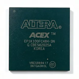
EP4CE75F23I8L - Cyclone IV E FPGA, 75K LE, 484-FBGA | Intel
MPN: EP4CE75F23I8L ✓ Active| Qty | Unit Price | Extended |
|---|---|---|
| 1 | $304.72 | $304.72 |
| 10 | $289.48 | $2,894.80 |
| 100 | $259.01 | $25,901.00 |
| 500 | $232.83 | $116,415.00 |
| 1,000 | $213.3 | $213,300.00 |
EP4CE75F23I8L Overview
A Field Programmable Gate Array (FPGA) is a semiconductor device built around an array of configurable logic blocks (CLBs), programmable interconnect, and embedded memory and DSP resources. FPGAs belong to the broader category of programmable logic devices (PLDs), sitting alongside CPLDs in the hierarchy of digital ICs; they differ from microcontrollers by implementing logic in hardware via parallel fabric rather than executing software on a sequential core. The Cyclone IV E family specifically targets cost-sensitive high-volume designs that previously used ASICs or ASSPs.
Key features of the EP4CE75F23I8L include 75,408 logic elements (~7.5K LE per kLE naming), 274 embedded 18x18 multipliers, 4 PLLs with dedicated outputs, and dedicated DDR/DDR2/QDR II memory controllers with PHY. The device supports LVDS, SSTL, HSTL, and LVPECL I/O standards, and offers a low static power architecture that consumes roughly one-third the power of the prior Cyclone III generation at comparable performance.
Technically, the Cyclone IV E is built on a 60 nm low-leakage process with a fixed routing architecture and 9-Kbit M9K memory blocks. It includes configuration support via passive serial, active serial (EPCS), JTAG, and Fast Passive Parallel modes. Bitstream encryption with AES 128-bit key is supported for IP protection.
Typical applications include industrial machine vision, motor control and factory automation, broadcast video processing, PCIe endpoint bridges, and cost-sensitive ASIC replacement. The wide I/O count and on-chip memory make it suitable for designs that previously required a discrete DSP plus microcontroller.
When designing with this part, plan clock distribution through the PLL blocks and respect the LVDS pair count per bank to avoid signal-integrity violations; the dedicated DDR PHY simplifies SDRAM interface design but requires matched-length routing. Industrial-grade temperature range (I8) suits outdoor or non-temperature-controlled enclosures.
This page synthesizes distributor pricing, drop-in same-family Cyclone IV E variants, and practical design notes that are not found in the bare manufacturer datasheet.
Drop-in alternatives for EP4CE75F23I8L — same package, pin-to-pin compatible. Different-package parts requiring PCB rework are excluded.
Variants in this series
Same-series models that are drop-in compatible with EP4CE75F23I8L (same form factor and footprint) — differing in Package, Embedded 18x18 Multipliers, Configuration Modes, Family, Embedded Memory (bits).
Quick Comparison Tool — Select alternative parts for side-by-side comparison:
EP4CE115F23I8LN
✅ Drop-In✓ In Stock
$198.75 / Unit
View Datasheet →EP4CE55F23I8L
✅ Drop-In✓ In Stock
$143.43 / Unit
View Datasheet →EP4CE40F23I8L
✅ Drop-In✓ In Stock
$79.5 / Unit
View Datasheet →EP4CE75F23I7N
✅ Drop-In ⚠️ 参数待验证✓ In Stock
$118 / Unit
View Datasheet →EP4CE75F23C8L
✅ Drop-In ⚠️ 参数待验证✓ In Stock
Contact for price
View Datasheet →EP4CE75F23I8L Maximum Ratings & Electrical Characteristics
| Family | Cyclone IV E |
| Logic Elements | 75,408 |
| Embedded Memory (bits) | 2,810,880 |
| Number of M9K Memory Blocks | 305 |
| Embedded 18x18 Multipliers | 274 |
| User I/O Pins | 292 |
| PLLs | 4 |
| Global Clock Networks | 20 |
| Maximum User I/O | 292 |
| Package | 484-ball FBGA |
| Operating Temperature | -40C to +85C (Industrial) |
| Supply Voltage (Core) | 1.0 V / 1.2 V |
| I/O Standards Supported | LVDS, SSTL, HSTL, LVPECL, LVCMOS, LVTTL |
| Configuration Modes | AS, PS, FPP, JTAG |
| Process Node | 60 nm low-leakage |
| RoHS Status | Compliant |
| MSL Level | 3 |
| Mounting Type | Surface Mount (BGA) |
EP4CE75F23I8L Pin Configuration
| Pin A1 | I/O — User I/O pin (bank 1A) |
| Pin B1 | I/O — User I/O pin (bank 1A) |
| Pin C1 | I/O — User I/O pin (bank 1A) |
| Pin D1 | VCCIO1A — I/O bank 1A supply |
| Pin E1 | I/O — User I/O pin |
| Pin F1 | I/O — User I/O pin |
| Pin G1 | VCCINT — Core supply (1.0V/1.2V) |
| Pin H1 | I/O — User I/O pin |
| Pin J1 | I/O — User I/O pin |
| Pin K1 | GND — Ground |
| Pin L1 | I/O — User I/O pin |
| Pin M1 | VCCIO1B — I/O bank 1B supply |
| Pin N1 | I/O — User I/O pin |
| Pin P1 | I/O — User I/O pin |
| Pin R1 | I/O — User I/O pin |
| Pin T1 | I/O — User I/O pin |
| Pin U1 | GND — Ground |
| Pin V1 | I/O — User I/O pin |
| Pin W1 | I/O — User I/O pin |
| Pin Y1 | I/O — User I/O pin |
| Pin AA1 | VCCIO2 — I/O bank 2 supply |
| Pin AB1 | I/O — User I/O pin |
| Pin AC1 | I/O — User I/O pin |
| Pin AD1 | I/O — User I/O pin |
| Pin AE1 | GND — Ground |
Typical Applications
EP4CE75F23I8L is suitable for 6 applications: Industrial Machine Vision, Multi-Axis Motor Control, PCIe Endpoint Bridge, Broadcast Video Processing, ASIC/ASSP Replacement, Test and Measurement Instrumentation.
Industrial Machine Vision
The EP4CE75F23I8L's 75,408 logic elements and 305 M9K memory blocks (2.8 Mbit total) deliver the throughput required for multi-camera machine vision pipelines. With 274 embedded 18x18 multipliers, the FPGA performs Sobel/Canny edge detection and Bayer demosaicing in hardware, sustaining 60 fps at 1080p resolution. The 4 PLLs drive pixel-clock and gigabit-Ethernet reference clocks simultaneously. Industrial-grade temperature range (-40C to +85C) lets the FPGA operate directly on the factory floor without a controlled enclosure.
Recommended
Multi-Axis Motor Control
In servo-drive and stepper-motor applications, the EP4CE75F23I8L provides the parallel DSP bandwidth needed for Field-Oriented Control (FOC) loops across multiple axes. Each FOC axis consumes roughly 4,000 LEs plus one 18x18 multiplier for the Park/Clarke transform; the EP4CE75 fits 4-6 axes with current-loop execution under 2 microseconds. The 292 user I/Os accept quadrature encoder feedback, Hall sensors, and PWM outputs without external muxing. Industrial temperature rating handles under-cabinet thermal stress.
Recommended
PCIe Endpoint Bridge
The EP4CE75F23I8L implements a PCIe Gen1 x1 or x4 endpoint using its soft IP and dedicated hard PCIe block. With 75K LEs, designers add protocol-aware logic on top of the PCIe hard IP for protocol bridging (PCIe-to-Ethernet, PCIe-to-Memory). The 2.8 Mbit embedded buffer memory holds DMA descriptors and packet payloads. The BGA package exposes the 4 PCIe lanes plus 4 PLLs for reference clock conditioning.
Recommended
Broadcast Video Processing
For SD/HD video routing and color-space conversion, the EP4CE75F23I8L delivers the parallelism needed for real-time 4:4:4 processing. The 305 M9K blocks provide line buffers up to 1080p; the 292 user I/Os accept HDMI/TMDS pairs directly with on-chip LVDS transceivers supporting SD/HD-SDI. Industrial temperature tolerance suits broadcast rack environments with limited airflow.
Recommended
ASIC/ASSP Replacement
The Cyclone IV E family is Intel's primary offering for low-cost ASIC replacement at volumes from 5K-500K units. The EP4CE75F23I8L hits the sweet spot where mask-charge NRE for a 90 nm ASIC exceeds FPGA unit-cost over the product lifetime. With Nios II soft-core support, designers integrate a 32-bit RISC processor alongside custom peripherals in the same fabric, replacing MCU-plus-ASIC systems on a single chip.
Recommended
Test and Measurement Instrumentation
The EP4CE75F23I8L serves as a reconfigurable logic analyzer or arbitrary waveform generator in bench-top instrumentation. The 75K LEs plus 274 multipliers enable real-time DSP for FFT-based spectrum analysis up to several MHz of bandwidth. The 292 user I/Os accept high-speed ADC/DAC parallel data buses; the 4 PLLs drive ADC sample clocks and DAC update clocks at independent rates. Industrial temperature rating is suitable for laboratory environments.
Recommended
Recommended Products Summary
Engineering reference data for EP4CE75F23I8L — comparison, design guidance, and compliance information.
Selection Guide
Comparison with Alternatives
| Parameter | This Product | EP4CE115F23I8LN | EP4CE55F23I8L | EP4CE40F23I8L | EP4CE75F23I7N | EP4CE75F23C8L |
|---|---|---|---|---|---|---|
| Brand | Intel | Intel | Intel | Intel | Intel | Intel |
| Package | 484-FBGA | 484-FBGA - same | 484-FBGA - same | 484-FBGA - same | 484-FBGA - same | 484-FBGA - same |
| Logic Elements | 75,408 | 114,480 | 55,560 | 39,600 | 75,408 | 75,408 |
| Embedded Memory (bits) | 2,810,880 | 3,981,312 | 2,340,000 | 1,134,000 | 2,810,880 | 2,810,880 |
| 18x18 Multipliers | 274 | 266 | 154 | 116 | 274 | 274 |
| User I/Os | 292 | 292 | 324 | 223 | 292 | 292 |
| Operating Temperature | -40C to +85C (I8) | -40C to +85C (I8) | -40C to +85C (I8) | -40C to +85C (I8) | 0C to +85C (I7) | 0C to +85C (C8) |
| Unit Price (qty 1, USD) | 304.72 | higher (higher density) | lower (lower density) | lowest (smallest density) | lower (commercial temp) | lower (slower speed grade) |
Key Differentiators
- Highest-density same-footprint drop-in upgrade path available (vs EP4CE115F23I8LN)
- Industrial temperature range as standard (vs EP4CE75F23I7N)
- Higher speed grade for timing-critical paths (vs EP4CE75F23C8L)
Design Notes
Estimated: at 100% logic utilization with all 4 PLLs active and typical toggle rate, core current draw is approximately 500-800 mA at 1.2V VCCINT. Use a switching regulator with at least 1.5A headroom (TPS54331 or equivalent). Decouple each VCCINT/VCCIO plane with 10uF bulk + 0.1uF + 0.01uF ceramic caps per the Cyclone IV E Hardware Reference. I/O banks require separate VCCIO rails - 8 banks on the 484-FBGA package.
The 484-FBGA uses a 1.0 mm ball pitch, which mandates 4-6 PCB layers with microvia or via-in-pad construction. Signal escape routing requires dog-bone fanouts from inner rows. Match differential pair lengths to within 150 mils for DDR2; the dedicated DDR PHY expects matched impedance of 50 ohm SE / 100 ohm diff. Intel's Cyclone IV E pin connection guidelines recommend keeping each differential pair within the same I/O bank.
Estimated: the FBGA-484 has theta_JA around 18 C/W with proper thermal via array under the package. Without thermal vias, expect junction-to-ambient above 30 C/W. Place a 4x4 via array (0.3mm drill, 1.0mm pitch) on the package center GND balls and connect to inner ground plane for adequate heat dissipation. Industrial temperature range (I8) still requires junction temperature below 100C for 10-year reliability.
Use EPCS16 or EPCS64 serial flash for Active Serial (AS) configuration mode - the bitstream for a 75% utilization EP4CE75F23I8L design fits in EPCS16 (16 Mbit). Enable AES-128 bitstream encryption via Quartus Programmer to protect IP. JTAG chain should include a 10K pull-up on TCK and TMS to allow boundary-scan without driving the pins.
Compliance Information
RoHS and REACH compliant per Intel/Altera product page. AEC-Q100 qualification not explicitly stated; for automotive AEC-Q100 applications consult Intel automotive-grade part numbers. Halogen-free status not confirmed in provided web data.