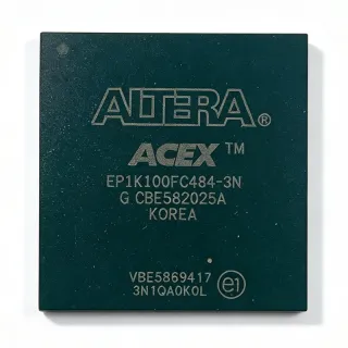
EP4CGX75CF23I8N - 73.9K LE Cyclone IV GX FPGA, 484-FBGA | Intel
MPN: EP4CGX75CF23I8N ✓ Active| Qty | Unit Price | Extended |
|---|---|---|
| 1 | $145 | $145.00 |
| 10 | $132.5 | $1,325.00 |
| 100 | $119.8 | $11,980.00 |
| 250 | $110.25 | $27,562.50 |
| 500 | $102.4 | $51,200.00 |
EP4CGX75CF23I8N Overview
A field-programmable gate array (FPGA) is a reconfigurable semiconductor device that lets designers implement custom digital logic, memory blocks, DSP pipelines, and high-speed I/O protocols after fabrication. The Cyclone IV GX family sits in the hierarchy of programmable logic devices (PLDs) -> FPGAs -> low-power FPGAs -> Cyclone series -> Cyclone IV generation -> Cyclone IV GX transceiver-equipped sub-family, offering an optimal balance of power, cost, and serial I/O for mainstream designs.
Key features include up to 290 maximum user I/O pins, eight integrated 3.125 Gbps transceivers (configurable as PCIe Gen1 x1/x2/x4 hard IP), 198 embedded 18x18 multipliers for DSP, and 4 PLL plus 4 DLL clock resources per device. The -I8 speed grade combined with the industrial -40C to +100C junction temperature rating makes this part suitable for harsh-environment and long-lifecycle embedded platforms.
The architecture pairs an SRAM-based 4-input look-up table (LUT) fabric with dedicated RAM blocks (M9K), DSP blocks, and hard PCIe/PLL/DLL silicon IP. With 4,257,792 embedded memory bits and 198 multipliers, the device supports high-throughput parallel DSP such as digital pre-distortion, baseband processing, and multi-channel video pipelines, while the 60 nm process keeps static and dynamic power well below competing 90/130 nm alternatives of similar density.
Typical applications span industrial machine vision, broadcast video processing, PCIe endpoint cards, motor control and factory automation, automotive driver assistance systems (telematics, rear-view camera aggregation), and communications backplane bridging. The integrated transceivers remove the need for external PHY devices when interfacing to SFP, GbE, CPRI, or PCIe peripherals.
When designing with this part, allocate decoupling capacitors near every VCCINT/VCCA/VCCD_PLL ball group, follow Intel's PCB layout guidelines for high-speed transceiver channels, and use the Quartus Prime design toolchain for synthesis, place-and-route, and timing closure. Confirm signal-integrity simulation of transceiver channels before committing to layout.
This page synthesizes manufacturer specifications, package pinout, drop-in compatible variants within the Cyclone IV GX family, and practical design notes not consolidated on the standard distributor product page.
Drop-in alternatives for EP4CGX75CF23I8N — same package, pin-to-pin compatible. Different-package parts requiring PCB rework are excluded.
Variants in this series
Same-series models that are drop-in compatible with EP4CGX75CF23I8N (same form factor and footprint) — differing in Package, Operating Temperature, Embedded Memory, Mounting Type, Logic Elements.
Quick Comparison Tool — Select alternative parts for side-by-side comparison:
EP4CGX75CF23I7N
✅ Drop-In✓ In Stock
$165.3 / Unit
View Datasheet →EP4CGX75CF23C8N
✅ Drop-In✓ In Stock
Contact for price
View Datasheet →EP4CGX75CF23C7N
✅ Drop-In✓ In Stock
$71.2 / Unit
View Datasheet →EP4CGX110CF23I7N
✅ Drop-In✓ In Stock
$1650.08 / Unit
View Datasheet →EP4CGX50CF23I8N
✅ Drop-In✓ In Stock
$54 / Unit
View Datasheet →EP4CE75F23I8N
✅ Drop-In📋 Reference alternative (not in catalog)
EP4CGX75CF23I8N Maximum Ratings & Electrical Characteristics
| Family | Cyclone IV GX |
| Logic Elements (LE) | 73,920 |
| Embedded Memory Bits | 4,257,792 |
| Embedded Memory Type | M9K blocks |
| Embedded Multipliers (18x18) | 198 |
| Maximum User I/O Pins | 290 |
| Transceivers | 8 channels up to 3.125 Gbps |
| PCIe Hard IP | 1 hard PCIe Gen1 block (x1/x2/x4) |
| PLLs | 4 |
| DLLs | 4 |
| Global Clock Networks | 20 |
| Process Technology | 60 nm |
| Core Voltage (VCCINT) | 1.2 V |
| Package | 484-ball FBGA |
| Package Code | F23 |
| Speed Grade | 8 (commercial fast) |
| Operating Junction Temperature | -40C to +100C (industrial) |
| RoHS Status | Compliant |
| Mounting Type | Surface Mount (BGA) |
| MSL Level | 3 |
EP4CGX75CF23I8N f23 Pin Configuration Guide
Pin configuration for EP4CGX75CF23I8N (f23 package). This digital IC includes GPIO, communication interfaces (UART, SPI, I2C), and power pins. Refer to the manufacturer datasheet for alternate pin functions and configuration options. Essential for embedded system design and PCB layout.

No detailed pinout data available for EP4CGX75CF23I8N.
Refer to the datasheet for full pin configuration.
Typical Applications
EP4CGX75CF23I8N is suitable for 7 applications: Industrial Machine Vision Systems, PCIe Endpoint Cards and Embedded Host Bridges, Broadcast Video Processing and Format Conversion, Automotive Telematics and Driver Assistance, Communications Backplane Bridging, Motor Control and Industrial Automation, Medical Imaging and Diagnostic Equipment.
Industrial Machine Vision Systems
Why EP4CGX75CF23I8N fits: The 73,920 logic elements combined with 198 embedded 18x18 multipliers and 4,257,792 bits of M9K memory deliver the parallel pixel-processing throughput required by multi-camera machine vision pipelines. The 3.125 Gbps transceivers can carry Camera Link, CoaXPress, or GigE Vision data directly from sensors to fabric without external PHY devices. How it is used: The FPGA performs image pre-processing (debayering, gamma, white balance) and feature extraction (edge detection, blob analysis) in real time, before forwarding summarized data to an industrial PC via PCIe Gen1 x4 using the integrated hard PCIe IP. The industrial -40C to +100C temperature rating enables deployment in factory-floor enclosures without additional thermal management.
Recommended
PCIe Endpoint Cards and Embedded Host Bridges
Why EP4CGX75CF23I8N fits: The integrated hard PCIe Gen1 IP block (configurable as x1/x2/x4) saves thousands of LEs and dramatically simplifies timing closure compared with soft PCIe implementations. The eight 3.125 Gbps transceivers also support sideband serial links (I2C-over-serializer, SPI bridges) common on embedded carrier cards. How it is used: The EP4CGX75CF23I8N functions as a PCIe endpoint exposing custom register interfaces, DMA engines, and IRQ logic to a host CPU. Combined with its 290 user I/Os and 4.2 Mbit of embedded memory, it can buffer large DMA transfers and aggregate data from multiple peripheral buses (USB, I2C, SPI, parallel) into a single high-bandwidth PCIe uplink to the host.
Recommended
Broadcast Video Processing and Format Conversion
Why EP4CGX75CF23I8N fits: With 198 DSP multipliers and 4.2 Mbit of on-chip memory, the device can sustain full-HD video at 60 fps for color-space conversion, scaling, deinterlacing, and chroma keying. The 290 user I/Os accommodate wide parallel video buses (16/24/32-bit) alongside audio, control, and ancillary data interfaces. How it is used: The FPGA ingests SDI or parallel video streams, performs real-time pixel-rate processing in the DSP fabric, and outputs HDMI, DisplayPort, or BT.1120. The transceivers can be used for 3G-SDI or HD-SDI input, eliminating external SDI deserializer chips. Industrial temperature rating ensures reliable operation in broadcast equipment racks with constrained cooling.
Recommended
Automotive Telematics and Driver Assistance
Why EP4CGX75CF23I8N fits: The industrial -40C to +100C junction rating and integrated transceivers support CAN-FD, FlexRay, Automotive Ethernet, and LVDS aggregation from multiple sensors (radar, camera, ultrasonic). The 198 multipliers handle real-time sensor fusion algorithms. How it is used: The FPGA aggregates rear-view, surround-view, and driver-monitoring camera data, performs object detection preprocessing, and forwards results to an automotive SoC over PCIe. Designers building production automotive platforms should evaluate AEC-Q100-qualified devices separately; this part is industrial-grade rather than full automotive-qualified.
Recommended
Communications Backplane Bridging
Why EP4CGX75CF23I8N fits: The eight 3.125 Gbps transceivers are ideal for bridging between backplane serial protocols such as CPRI, OBSAI, SGMII, and 1G/2.5G Ethernet, supporting up to 25 Gbps aggregate serial bandwidth. The 73,920 LEs and 4.2 Mbit of memory buffer protocol conversion at line rate. How it is used: The FPGA terminates incoming serial lanes, decodes protocol headers, performs address translation or rate adaptation in the fabric using embedded M9K memory as packet buffers, and re-transmits on outgoing lanes. Industrial temperature rating supports outdoor base-station and small-cell deployments.
Recommended
Motor Control and Industrial Automation
Why EP4CGX75CF23I8N fits: The combination of 198 DSP multipliers, 290 user I/Os, and the 60 nm low-power process delivers deterministic multi-axis motor control loops while keeping junction temperatures low. The transceivers support industrial Ethernet protocols (EtherCAT, PROFINET) at 100 Mbit/s over LVDS or 1 Gbit/s over SGMII. How it is used: The FPGA runs field-oriented control (FOC), space-vector PWM, and current/voltage sampling loops for multi-axis servo drives. Encoder interfaces (EnDat, BiSS, SSI) are implemented in fabric using the M9K memory blocks. The industrial temperature rating supports cabinet-mounted drives in factory environments.
Recommended
Medical Imaging and Diagnostic Equipment
Why EP4CGX75CF23I8N fits: 198 multipliers and 4.2 Mbit of embedded memory enable real-time ultrasound beamforming, FFT-based Doppler processing, and image reconstruction algorithms. The integrated transceivers support high-speed ADC data interfaces (LVDS, JESD204B via soft logic) for modern medical imaging front-ends. How it is used: The FPGA aggregates digitized transducer channels, performs delay-and-sum beamforming in fabric, runs envelope detection and log compression, and outputs processed video to a host PC or display controller. Designers should verify IEC 60601 and IEC 62304 compliance separately; this part provides the hardware substrate but does not by itself constitute a medical-certified subsystem.
Recommended
Recommended Products Summary
Engineering reference data for EP4CGX75CF23I8N — comparison, design guidance, and compliance information.
Selection Guide
Comparison with Alternatives
| Parameter | This Product | EP4CGX75CF23I7N | EP4CGX75CF23C8N | EP4CGX75CF23C7N | EP4CGX110CF23I7N | EP4CGX50CF23I8N | EP4CE75F23I8N |
|---|---|---|---|---|---|---|---|
| Brand | Intel (Altera) | Intel (Altera) | Intel (Altera) | Intel (Altera) | Intel (Altera) | Intel (Altera) | Intel (Altera) |
| Package | 484-ball FBGA (F23) | 484-ball FBGA (F23) - same | 484-ball FBGA (F23) - same | 484-ball FBGA (F23) - same | 484-ball FBGA (F23) - same | 484-ball FBGA (F23) - same | 484-ball FBGA (F23) - same |
| Logic Elements | 73,920 | 73,920 | 73,920 | 73,920 | 109,440 | 49,888 | 75,408 |
| Embedded Memory (bits) | 4,257,792 | 4,257,792 | 4,257,792 | 4,257,792 | 5,490,048 | 2,560,000 | 2,810,880 |
| Embedded Multipliers (18x18) | 198 | 198 | 198 | 198 | 280 | 140 | 200 |
| Transceivers | 8 (up to 3.125 Gbps) | 8 (up to 3.125 Gbps) | 8 (up to 3.125 Gbps) | 8 (up to 3.125 Gbps) | 8 (up to 3.125 Gbps) | 8 (up to 3.125 Gbps) | 0 (none) |
| PCIe Hard IP | 1 (Gen1 x1/x2/x4) | 1 (Gen1 x1/x2/x4) | 1 (Gen1 x1/x2/x4) | 1 (Gen1 x1/x2/x4) | 1 (Gen1 x1/x2/x4) | 1 (Gen1 x1/x2/x4) | 0 (none) |
| Speed Grade | 8 | 7 | 8 | 7 | 7 | 8 | 8 |
| Operating Temperature | -40C to +100C (industrial) | -40C to +100C (industrial) | 0C to +85C (commercial) | 0C to +85C (commercial) | -40C to +100C (industrial) | -40C to +100C (industrial) | -40C to +100C (industrial) |
| Process / Core Voltage | 60 nm / 1.2 V | 60 nm / 1.2 V | 60 nm / 1.2 V | 60 nm / 1.2 V | 60 nm / 1.2 V | 60 nm / 1.2 V | 60 nm / 1.2 V |
Key Differentiators
- Industrial temperature rating with speed grade 8 (vs EP4CGX75CF23C8N)
- Same-die drop-in with faster Fmax (vs EP4CGX75CF23I7N)
- Logic capacity upgrade path within same footprint (vs EP4CGX110CF23I7N)
- Lower-cost drop-in for non-transceiver designs (vs EP4CE75F23I8N)
- Integrated hard PCIe Gen1 IP block (vs Soft PCIe cores on competing FPGAs)
Design Notes
Estimated: At 73,920 LEs, 198 multipliers, 8 transceivers at 3.125 Gbps, and 4 PLLs simultaneously active, the EP4CGX75CF23I8N consumes approximately 1.5-2.5 W dynamic power plus 100-300 mW static. Provide independent decoupling networks for VCCINT (1.2 V core), VCCA (2.5 V PLL analog), VCCD_PLL (1.2 V PLL digital), and each transceiver channel supply. Place one 0.1 uF X7R ceramic plus one 10 uF bulk per supply pin group. Refer to the Intel Cyclone IV GX device datasheet power section for measured quiescent and dynamic power budgets by configuration.
The 484-ball FBGA at 1.0 mm pitch requires 4-6 layer PCB with microvia or via-in-pad construction. Route all transceiver differential pairs with 100 ohm differential impedance, length-matched to within 150 mils, and maintain continuous reference plane on layer 2 or layer 3. Transceiver channels are highly sensitive to impedance discontinuities and crosstalk - simulate channel S-parameters with the Intel-provided IBIS-AMI models before committing to layout. Avoid routing high-speed signals across plane splits or under noisy power regions.
Place configuration flash and configuration mode jumpers (MSEL pins) within 2 inches of the FPGA. For JTAG boundary-scan programming, add a 10-pin header compatible with the Intel USB-Blaster or compatible third-party programmers. Reserve a complete ground ring around the BGA and stitch via fence every 200 mils around the device outline. Route all global clock networks on inner layers with controlled impedance and shield them with adjacent ground planes to minimize skew.
Transceiver channels operating at 3.125 Gbps require AC-coupling capacitors (typically 100 nF X7R) in series with each TX and RX lane. The reference clock input requires a low-jitter LVDS or LVPECL source with jitter below the receiver's tolerance budget (typically < 1 ps RMS for 3.125 Gbps links). Use Intel's Cyclone IV GX Transceiver Toolkit within Quartus Prime to validate bit-error-rate (BER) performance and eye-diagram margin on prototype hardware before finalizing the PCB.
Estimated: The FBGA package has a theta_JA of approximately 12 C/W with a standard 4-layer JEDEC test board. At 2.5 W total power dissipation, junction temperature rise above ambient is about 30 C - manageable without a heatsink in well-ventilated enclosures. For sealed industrial cabinets or > 85 C ambient, recommend a small heatsink or thermal pad assembly to keep junction below 100 C. Forced-air cooling (1-2 m/s) further reduces junction temperature by 10-20 C. Always validate thermal performance with the actual enclosure and workload profile.
Compliance Information
RoHS compliant per Intel Altera product declaration. Industrial temperature range -40C to +100C junction. AEC-Q100 not qualified - this part is industrial-grade, not full automotive-qualified. For full AEC-Q100 requirements, consult Intel automotive-grade FPGA portfolio separately. Halogen-free status: refer to the latest Intel material declaration for verification.