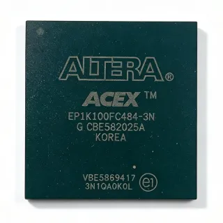
EP3C16F484C7N - Cyclone III FPGA, 15K LEs, 484-FBGA | Intel
MPN: EP3C16F484C7N ✓ Active| Qty | Unit Price | Extended |
|---|---|---|
| 1 | $53.18 | $53.18 |
| 10 | $48.5 | $485.00 |
| 100 | $42.9 | $4,290.00 |
| 500 | $36.25 | $18,125.00 |
| 1,000 | $30.1 | $30,100.00 |
EP3C16F484C7N Overview
A Field-Programmable Gate Array (FPGA) is a programmable logic device that allows engineers to implement arbitrary digital circuits after PCB fabrication. FPGAs sit in the programmable logic hierarchy above simple PLDs and below ASICs, bridging the gap between fixed-function ICs and full-custom silicon. The Cyclone III family in particular targets cost-sensitive, high-volume applications where the per-board BOM cost of a traditional FPGA would be prohibitive, while still offering DSP blocks, on-chip RAM, and high-speed serial capability for parallel digital processing.
Key features of the EP3C16F484C7N include 346 LVDS-capable user I/O pins arranged across eight I/O banks, configurable LVDS/LVCMOS/LVTTL support, and dedicated hardware multipliers (up to 56 18x18) for DSP pipelines. The device supports JTAG (IEEE 1149.1) boundary-scan configuration via the EPCS serial configuration device family, plus 4 PLLs for clock synthesis. Speed grade -7 places this part in the mid-performance bin of the Cyclone III family.
Cyclone III architecture combines look-up tables (LUTs), embedded memory blocks (M9K), DSP blocks, and routing fabric. The 65 nm process node reduces static leakage versus the prior Cyclone generation, enabling the family to operate with typical power well under 0.5 W for many designs. Cyclone III is widely used in industrial control, motor drive, video processing, and prototyping applications.
Typical applications include industrial machine vision, motor control and drive interfaces, low-cost video bridging, LED wall controllers, software-defined radio (SDR) front ends, and ASIC/SoC prototyping. The combination of DSP blocks and a generous logic budget makes the EP3C16F484C7N especially suited to DSP-centric embedded designs.
When designing with this device, validate thermal performance for your specific I/O switching profile and ensure the configuration scheme (EPCS flash or JTAG) is provisioned in your PCB layout. Speed grade -7 provides balanced timing margin; faster -8 grades are not stocked for this part number.
Drop-in alternatives for EP3C16F484C7N — same package, pin-to-pin compatible. Different-package parts requiring PCB rework are excluded.
Variants in this series
Same-series models that are drop-in compatible with EP3C16F484C7N (same form factor and footprint) — differing in Package, Process Technology, Core Voltage, Embedded Memory, Operating Temperature.
Quick Comparison Tool — Select alternative parts for side-by-side comparison:
EP3C16F484C8N
✅ Drop-In✓ In Stock
$29.95 / Unit
View Datasheet →EP3C16F484I7N
✅ Drop-In✓ In Stock
$36.4 / Unit
View Datasheet →EP3C16F484C6N
✅ Drop-In✓ In Stock
$38.4 / Unit
View Datasheet →EP3C25F484C7N
✅ Drop-In ⚠️ 参数待验证📋 Reference alternative (not in catalog)
EP3C10F484C8N
✅ Drop-In ⚠️ 参数待验证📋 Reference alternative (not in catalog)
EP3C16F484C7N Maximum Ratings & Electrical Characteristics
| Device Family | Cyclone III |
| Logic Elements | 15,408 |
| Embedded Memory | 504 Kbits (M9K blocks) |
| Embedded Multipliers | 56 (18x18) |
| PLLs | 4 |
| User I/O Pins | 346 |
| Process Technology | 65 nm TSMC low-power |
| Core Voltage | 1.2 V (1.15 V to 1.25 V) |
| Package | 484-ball FBGA |
| Speed Grade | -7 |
| Operating Temperature | 0C to +85C (commercial) |
| Maximum Internal Frequency | 437.5 MHz |
| I/O Standards Supported | LVDS, LVCMOS, LVTTL, SSTL, HSTL |
| Configuration Method | JTAG (IEEE 1149.1), EPCS serial flash, Active Serial |
| RoHS Status | Compliant |
EP3C16F484C7N 484-ball fbga Pin Configuration Guide
Pin configuration for EP3C16F484C7N (484-ball fbga package). This digital IC includes GPIO, communication interfaces (UART, SPI, I2C), and power pins. Refer to the manufacturer datasheet for alternate pin functions and configuration options. Essential for embedded system design and PCB layout.

No detailed pinout data available for EP3C16F484C7N.
Refer to the datasheet for full pin configuration.
Typical Applications
EP3C16F484C7N is suitable for 6 applications: Industrial Motor Control, Machine Vision and Image Processing, LED Video Wall Controller, Software-Defined Radio (SDR) Front End, ASIC and SoC Prototyping, Automotive Infotainment Test Bench.
Industrial Motor Control
The EP3C16F484C7N's 15,408 logic elements, 56 hardware 18x18 multipliers, and 346 user I/O pins make it a strong fit for industrial motor control applications such as field-oriented control (FOC) of three-phase PMSM and AC induction drives. The DSP blocks implement Clarke/Park transforms and PI loops at high update rates, while the abundant LVDS-capable I/O directly interfaces to incremental encoder feedback and resolver-to-digital converter chips. Four on-chip PLLs synthesize motor PWM carrier frequencies and resolver excitation clocks from a single crystal. Compared to an MCU, the FPGA parallelizes the control law and current sampling, lowering loop latency below 1 microsecond for high-dynamic servo drives.
Recommended
Machine Vision and Image Processing
The EP3C16F484C7N is well suited to industrial machine vision pipelines, supporting parallel Bayer demosaicing, Sobel edge detection, and thresholding across a 1080p60 video stream. Its 504 Kbits of M9K embedded memory buffer line-scan rows, while the 56 hardware multipliers accelerate convolution kernels without consuming general-purpose logic. With 346 user I/O pins, the device can connect to MIPI-CSI2 deserializer chips, LVDS camera link receivers, and DDR2/DDR3 frame buffers simultaneously. Quartus II's VIP suite and reference designs shorten time-to-prototype for vision OEMs compared with a DSP-only approach.
Recommended
LED Video Wall Controller
For LED video wall controllers, the EP3C16F484C7N provides 346 LVDS-capable I/O pins to drive hub-75E panels directly, eliminating an external row/column buffer. Each LED wall tile requires 13 data lines plus clock and latch, so 346 I/O supports multiple tiles in parallel for higher refresh rates. The Cyclone III's 504 Kbits of on-chip RAM and 56 multipliers handle color-space conversion, brightness compensation, and gamma correction in real time. Designers often use the device's four PLLs to generate pixel clocks for several scan-rate zones of the wall while a single global refresh synchronizes the display.
Recommended
Software-Defined Radio (SDR) Front End
The EP3C16F484C7N serves as a digital down-conversion (DDC) front end in narrowband SDR designs, supporting digital mixing, decimation, and channelization between an ADC and a host processor. Its 56 dedicated 18x18 multipliers handle complex I/Q FFTs and FIR filters, while 504 Kbits of M9K memory stages decimation filters and re-samplers. Four PLLs synthesize the ADC sampling clock and a DSP baseband clock from a single reference, simplifying BOM. Compared to a fixed-function DDC ASIC, the Cyclone III gives the SDR platform frequency agility across multiple waveforms and standards.
Recommended
ASIC and SoC Prototyping
The EP3C16F484C7N is widely used as a low-cost ASIC prototyping platform, emulating custom logic and bus architectures before tape-out. With 15,408 logic elements and 504 Kbits of block RAM, designers can fit complex peripheral sets such as DDR controllers, custom DMA engines, and glue logic. Quartus II's synthesis, place-and-route, and incremental compilation flows let engineers iterate on RTL quickly, while the 484-FBGA package supports high-speed DDR2/DDR3 memory interfaces for prototype SoC verification. Larger Cyclone III and Stratix II devices are available for partitioning bigger ASIC RTL across multiple FPGAs.
Recommended
Automotive Infotainment Test Bench
Although the EP3C16F484C7N itself is a commercial-temperature part, it is commonly used on automotive infotainment development benches for protocol bridging and pre-silicon validation. The device's LVDS and LVCMOS I/O bridge LVDS camera links, MOST bus nodes, and CAN/LIN traffic into a development host. Designers route multiple automotive protocols into the FPGA, then verify stack behavior before the production MCU arrives. For in-vehicle deployment the EP3C16F484I7N industrial variant is recommended when the test bench sees under-hood or dashboard temperatures.
Recommended
Recommended Products Summary
Engineering reference data for EP3C16F484C7N — comparison, design guidance, and compliance information.
Selection Guide
Comparison with Alternatives
| Parameter | This Product | EP3C16F484C8N | EP3C16F484I7N | EP3C16F484C6N | EP3C25F484C7N | EP3C10F484C8N |
|---|---|---|---|---|---|---|
| Brand | Intel (Altera) | Intel (Altera) | Intel (Altera) | Intel (Altera) | Intel (Altera) | Intel (Altera) |
| Package | 484-FBGA | 484-FBGA - same | 484-FBGA - same | 484-FBGA - same | 484-FBGA - same | 484-FBGA - same |
| Logic Elements | 15,408 | 15,408 | 15,408 | 15,408 | 24,624 | 10,320 |
| Speed Grade | -7 | -8 (slower) | -7 (same) | -6 (faster) | -7 (same) | -8 (slower) |
| Operating Temperature | 0C to +85C (commercial) | 0C to +85C | -40C to +100C (industrial) | 0C to +85C | 0C to +85C | 0C to +85C |
| Embedded Memory | 504 Kbits | 504 Kbits | 504 Kbits | 504 Kbits | 594 Kbits | 423 Kbits |
| Embedded Multipliers (18x18) | 56 | 56 | 56 | 56 | 66 | 46 |
| User I/O Pins | 346 | 346 | 346 | 346 | 346 | 346 |
| PLLs | 4 | 4 | 4 | 4 | 4 | 4 |
Key Differentiators
- Speed grade -7 mid-performance bin (vs EP3C16F484C8N)
- Commercial temperature pricing advantage (vs EP3C16F484I7N)
- Balanced logic density for medium-complexity designs (vs EP3C25F484C7N)
- 346 high-density I/O exceeds typical Cyclone III 144-pin/256-pin variants (vs EP3C16F256I7N)
Design Notes
Estimated: The EP3C16F484C7N requires 1.2 V core, 2.5 V analog PLL, and per-bank VCCIO supplies. With all 346 I/O switching at 100 MHz, typical core current per Cyclone III handbook guidance is in the 0.5-1.0 A range. Bulk-decouple each VCCIO bank with a 10 uF ceramic plus 0.1 uF bypass per 10-15 I/O pins, and place a ferrite or pi filter on the 2.5 V PLL analog rail to minimize jitter. Decoupling close to the package minimizes switching-induced ground bounce on the 484-FBGA.
The 484-FBGA uses a 1.0 mm pitch ball array, which demands 4-6 layer PCB with microvia stacks to fan out cleanly. Match all LVDS pairs within 0.13 mm and route each pair to within 90 ohms differential impedance. Per Cyclone III pin connection guidelines, leave unused I/O pins floating rather than connecting to ground, because internal biasing makes tied-low pins a leakage path. Provide a complete GND pour under the BGA for thermal spreading.
Use an EPCS4 or EPCS16 serial configuration flash in Active Serial (AS) mode for production; the MSEL[2:0] pins must be tied to 010b for standard AS or to 000b for JTAG-only development. According to the Cyclone III handbook, the nCONFIG pin must be pulled high through a 10 kohm resistor and the nSTATUS pin must be left open. Place the EPCS flash within 100 mm of the FPGA to avoid signal-integrity issues on the DATA line.
Avoid driving LVDS pairs before the FPGA is fully configured, or output contention can damage adjacent buffers. Verify the JTAG chain order in advance using the Quartus II Chain Debugger; adding bypass resistors on TCK/TMS/TDO keeps the chain alive when the FPGA is not yet programmed. Do not hot-plug the 1.2 V core supply during AS configuration or the CRC error flag will trip. Finally, use the Quartus II PowerPlay estimator early to verify thermal headroom.
Compliance Information
RoHS and lead-free status confirmed via distributor listings. Cyclone III family is not AEC-Q100 qualified; for AEC-Q100 automotive work consider the Cyclone IV or Cyclone V families.