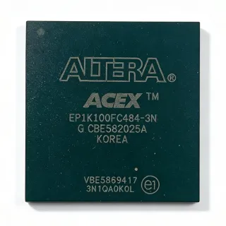
EP2C50F484C7 - Cyclone II FPGA, 50K LE, 484-FBGA | Intel
MPN: EP2C50F484C7 ✓ Active| Qty | Unit Price | Extended |
|---|---|---|
| 1 | $254.2 | $254.20 |
| 10 | $228.78 | $2,287.80 |
| 100 | $203.36 | $20,336.00 |
| 500 | $178 | $89,000.00 |
| 1,000 | $165 | $165,000.00 |
EP2C50F484C7 Overview
A Cyclone II FPGA is a SRAM-based programmable logic device that combines lookup-table-based logic blocks with embedded memory, embedded multipliers (DSP blocks), and phase-locked loops on a single die. In the broader system hierarchy, an FPGA sits below application-specific standard products (ASSPs) and above discrete logic gates, offering hardware-level parallelism that microcontrollers and DSPs cannot match. Designers use Cyclone II devices when time-to-market, design flexibility, or parallel signal processing outweigh the per-unit cost advantage of a hard-wired ASIC.
Key features of the EP2C50F484C7 include 50,528 logic elements (LEs), 129 M4K RAM blocks (594 Kbit total), 86 embedded 18 x 18 multipliers, four PLLs, and 294 maximum user I/Os. The 484-FBGA package supports a wide range of single-ended I/O standards (LVTTL, LVCMOS, SSTL, HSTL) plus differential standards (LVDS, RSDS, mini-LVDS, LVPECL) on selected pins, giving designers flexibility to bridge legacy and modern ASIC/ASSP interfaces.
The Cyclone II architecture uses a four-input LUT as the basic logic element, with a dedicated carry chain for fast arithmetic and a dedicated register per LE. Embedded multipliers are arranged in columns along the device, allowing DSP functions such as FIR filters and FFT butterflies to run at the full 402 MHz internal clock rate. The four PLLs provide clock multiplication, division, phase shifting, and duty-cycle control, which simplifies multi-clock-domain designs and reduces external clock-tree complexity.
Typical applications include industrial motor control and factory-automation backplanes, video-processing and image-pipeline front-ends, telecom line cards, low-cost software-defined radio prototyping, and PCI Express endpoint bridging. The 484-FBGA package makes the part suitable for board designs that need the highest I/O count in the Cyclone II family without stepping up to the larger Cyclone III/IV generations.
Designers should pay close attention to power-plane decoupling (multiple 0.1 uF and 10 uF caps near each VCC/GAT pair), JTAG chain ordering when multiple Altera/Intel devices share a bus, and configuration-mode selection between AS, PS, and JTAG. The device also requires a configuration flash or download cable for SRAM-based bitstream loading on every power-up.
This page combines distributor pricing, drop-in compatible alternatives in the same 484-FBGA footprint, and practical design notes not found in the standalone manufacturer datasheet, helping engineers select and source the EP2C50F484C7 with confidence.
Drop-in alternatives for EP2C50F484C7 — same package, pin-to-pin compatible. Different-package parts requiring PCB rework are excluded.
Variants in this series
Same-series models that are drop-in compatible with EP2C50F484C7 (same form factor and footprint) — differing in Package, Speed Grade, Operating Temperature, Process Technology, Configuration Modes.
Quick Comparison Tool — Select alternative parts for side-by-side comparison:
EP2C50F484C6
✅ Drop-In✓ In Stock
$110 / Unit
View Datasheet →EP2C50F484C6N
✅ Drop-In✓ In Stock
$180.47 / Unit
View Datasheet →EP2C50F484C8N
✅ Drop-In✓ In Stock
$68.2 / Unit
View Datasheet →EP2C35F484C7
✅ Drop-In✓ In Stock
$54.25 / Unit
View Datasheet →EP2C35F484C8
✅ Drop-In✓ In Stock
$28.9 / Unit
View Datasheet →EP2C35F484C7N
✅ Drop-In✓ In Stock
$85.2 / Unit
View Datasheet →EP2C50F484C7 Maximum Ratings & Electrical Characteristics
| Series | Cyclone II |
| Family | Cyclone II FPGA |
| Logic Elements | 50,528 |
| Total RAM Bits | 594,432 |
| Embedded Multipliers | 86 (18 x 18) |
| Number of PLLs | 4 |
| Maximum User I/O | 294 |
| Core Voltage | 1.2 V |
| Process Technology | 90 nm |
| Package | 484-ball FBGA |
| Package Code | BGA |
| Mounting Type | Surface Mount |
| Operating Temperature Range | Commercial (0C to +85C) - inferred from speed grade C7 |
| Speed Grade | C7 |
| Configuration Modes | AS, PS, JTAG |
EP2C50F484C7 bga Pin Configuration Guide
Pin configuration for EP2C50F484C7 (bga package). This digital IC includes GPIO, communication interfaces (UART, SPI, I2C), and power pins. Refer to the manufacturer datasheet for alternate pin functions and configuration options. Essential for embedded system design and PCB layout.

No detailed pinout data available for EP2C50F484C7.
Refer to the datasheet for full pin configuration.
Typical Applications
EP2C50F484C7 is suitable for 6 applications: Industrial Motor Control & Factory Automation, Video Processing & Image Pipeline, Telecom Line Cards & Baseband Processing, Software-Defined Radio Prototyping, PCI Express Endpoint Bridging & I/O Expansion, Development Boards & Education Platforms.
Industrial Motor Control & Factory Automation
The EP2C50F484C7's 50,528 logic elements and 86 embedded 18x18 multipliers make it a strong fit for multi-axis industrial motor control and factory-automation backplanes. Each axis typically requires PID loops, space-vector PWM generators, encoder quadrature decoders, and fault-handling state machines - easily fitting within ~3,000 LEs per axis, so the EP2C50F484C7 can drive up to 12-15 axes from a single device. The 294 user I/Os connect directly to incremental encoder inputs, Hall sensors, gate drivers, and isolated fieldbus interfaces (EtherCAT, Profibus, RS-485) without external bus switches. Designers typically configure the 4 on-chip PLLs to generate independent PWM frequencies (4-32 kHz) per axis with deterministic phase relationships.
Recommended
Video Processing & Image Pipeline
The EP2C50F484C7 is well-suited for mid-resolution video pipeline front-ends such as SD/HD video scaling, de-interlacing, color-space conversion, and on-screen-display overlay. With 594 Kbit of embedded RAM, the device can buffer multiple full video lines and implement line-store based algorithms like 3:2 pulldown and noise reduction. The 86 dedicated 18x18 multipliers enable real-time 2D convolution and edge-detection filters at pixel-clock rates up to 148 MHz, sufficient for 720p60 video. The 484-FBGA package exposes enough I/O for parallel RGB/YCbCr buses plus HSYNC/VSYNC and I2C control to typical LCD controller ASICs.
Recommended
Telecom Line Cards & Baseband Processing
The EP2C50F484C7 can be deployed in telecom line cards for low-density baseband signal processing, packet classification, and protocol bridging. Its 594 Kbit embedded RAM is sufficient to buffer ATM/Ethernet cells or implement small lookup tables for routing, while the 86 multipliers support chip-rate processing and convolutional FEC decoding in software-defined access equipment. The 484-FBGA package supplies 294 user I/Os to bond out parallel LVDS links to network processors, framer ASICs, and SERDES devices without an external bus expander. PCI-compatible I/O banks enable direct connection to PowerPC or MIPS-based control processors.
Recommended
Software-Defined Radio Prototyping
The EP2C50F484C7 is widely used as a prototyping platform for software-defined radio (SDR) baseband processing. With 86 embedded 18x18 multipliers and ~50K LEs, the device can implement multi-tap FIR filters, FFT/iFFT engines, digital up/down-converters, and symbol-mapper/demapper blocks for narrow-band waveforms (GSM, DVB, LTE uplink). The 4 PLLs provide independent sample-rate clocks for ADC/DAC interfaces, while the differential I/O pins support LVDS connections to high-speed converters. Quartus II reference designs and university SDR curricula use this exact part as a teaching and verification vehicle.
Recommended
PCI Express Endpoint Bridging & I/O Expansion
The EP2C50F484C7 supports PCI Express endpoint operation via external PHY plus an Altera-provided soft IP core, making it a cost-effective bridge between PCIe and legacy parallel buses such as PCI, ISA, or proprietary local buses. The 50K LEs comfortably host the PIPE interface, transaction layer, and data-path FIFOs, while 294 I/Os connect to the legacy bus and side-band signals (interrupts, GPIOs, I2C). 484-FBGA gives PCB designers the I/O headroom needed for x1 or x4 PCIe plus a full 32-bit/66 MHz parallel bus on the same device.
Recommended
Development Boards & Education Platforms
The EP2C50F484C7 is a common heart of university FPGA curriculum boards and Altera/Intel Cyclone II starter kits (such as the Cyclone II EP2C35/EP2C50 dev board family). Its 484-FBGA package exposes enough LEDs, switches, seven-segment displays, and expansion headers to support teaching labs covering state machines, CPU cores, VGA controllers, and audio processing. The Quartus II Web Edition toolchain has been free for this device for years, and a rich ecosystem of example projects (Nios II soft CPU, RISC-V soft cores, SoC labs) is publicly available, making the part a pedagogical workhorse.
Recommended
Recommended Products Summary
Engineering reference data for EP2C50F484C7 — comparison, design guidance, and compliance information.
Selection Guide
Comparison with Alternatives
| Parameter | This Product | EP2C50F484C6 | EP2C50F484C6N | EP2C50F484C8N | EP2C35F484C7 |
|---|---|---|---|---|---|
| Package | 484-FBGA (F484) | 484-FBGA - same | 484-FBGA - same | 484-FBGA - same | 484-FBGA - same |
| Brand | Intel (formerly Altera) | Intel - same | Intel - same | Intel - same | Intel - same |
| Logic Elements | 50,528 | 50,528 | 50,528 | 50,528 | 33,216 (~34% less) |
| Total RAM Bits | 594,432 | 594,432 | 594,432 | 594,432 | 483,840 |
| Embedded Multipliers (18x18) | 86 | 86 | 86 | 86 | 70 (~19% fewer) |
| PLLs | 4 | 4 | 4 | 4 | 4 |
| Max User I/O | 294 | 294 | 294 | 294 | 322 (larger I/O count) |
| Speed Grade | -7 | -6 (faster) | -6 (faster) | -8 (faster) | -7 (same) |
| Temperature Grade | Commercial (0C to +85C) | Commercial | Commercial, lead-free | Industrial (-40C to +100C), lead-free | Commercial |
Key Differentiators
- Highest logic density in the Cyclone II family below the EP2C70 (vs EP2C35F484C7)
- Same die across C6/C7/C8 speed grades simplifies inventory (vs EP2C50F484C6)
- 294 user I/Os enables dense parallel-bus bridging (vs EP2C50F484C6N)
Design Notes
Cyclone II EP2C50 devices draw up to ~1.5 W quiescent and substantially more under high toggle rates. Decouple each VCCINT (1.2 V) and VCCIO (per-bank) ball group with a 0.1 uF X7R ceramic plus a bulk 10 uF tantalum or polymer capacitor placed within 5 mm of the BGA. Use at least four-layer PCB with continuous power and ground planes; a six-layer stack-up is recommended for designs switching >100 MHz clocks to suppress SSN.
The 484-FBGA has a 1.0 mm ball pitch, requiring laser-drilled or 0.4 mm-pitch vias on the top layer with microvia stack-up if available. Route differential pairs (LVDS, RSDS) with 100 ohm differential impedance and length-matching to within 150 mil. Keep all configuration pins (MSEL, nCE, nCONFIG, nSTATUS, CONF_DONE, DCLK) routed short and isolated from switching I/O to avoid bitstream-loading glitches during AS or PS configuration.
Do not assume Cyclone II EP2C50 is hot-swappable at the I/O level unless all I/O banks are powered and IOH/IOH clamp diodes are accounted for. Cyclone II supports hot-socketing on most I/O, but VCCIO must sequence within datasheet limits or latch-up may occur. Also verify Quartus II version compatibility - bitstreams generated for newer Cyclone families will not load on Cyclone II silicon even if pin-compatible at the package level.
The EP2C50F484C7 484-FBGA has theta_JA of approximately 15 C/W with a properly designed 4-layer PCB. Under worst-case commercial operating conditions (85C ambient, high toggle rate, 1.2 V VCCINT), designers should budget <1.0 W continuous dissipation or apply forced-air cooling to keep junction temperature below 100C. The exposed thermal pad is not present on this package - thermal relief relies entirely on via-in-pad to internal planes.
Compliance Information
RoHS/REACH/lead-free status not provided in verified web data; check manufacturer product page for latest compliance certificates. The EP2C50F484C7 is commercial-grade (not AEC-Q100).