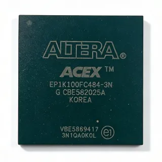
EP3CLS150F484C8 - 150K LE Cyclone III LS FPGA, 484-FBGA | Intel
MPN: EP3CLS150F484C8 ✗ End of Life| Qty | Unit Price | Extended |
|---|---|---|
| 1 | $165 | $165.00 |
| 10 | $152 | $1,520.00 |
| 100 | $138.5 | $13,850.00 |
| 250 | $128 | $32,000.00 |
| 500 | $119 | $59,500.00 |
EP3CLS150F484C8 Overview
An FPGA (Field-Programmable Gate Array) is a semiconductor device containing configurable logic blocks (CLBs), programmable interconnects, embedded memory, and DSP blocks that can be re-programmed by the designer after manufacture. FPGAs belong to the broader category of programmable logic devices (PLDs) and bridge the gap between fixed-function ASICs and software-defined processing. The Cyclone III LS family specifically targets low-static-power applications that previously required discrete glue logic or low-density ASICs.
Key features include 150,848 logic elements, 6137856 bits (about 6.14 Mbit) of embedded SRAM, four phase-locked loops (PLLs), and high-speed LVDS I/O support. The device also integrates dedicated hardware multipliers for DSP, a configuration controller supporting multiple boot modes (including external flash and JTAG), and security features such as configuration bitstream encryption via AES. Operating junction temperature is 0 C to 85 C (commercial grade).
The Cyclone III LS architecture uses an SRAM-based configuration cell and a low-k 65 nm process, which reduces dynamic power by roughly 50 percent compared to the prior-generation Cyclone II family. The 484-ball FBGA package exposes 8 dedicated clock/PLL pins, multi-standard I/O banks that support LVCMOS, LVTTL, SSTL, and LVDS signaling, and a footprint compatible with the wider Cyclone III LS density ladder (EP3C5/16/25/40/55/80/120/150).
Typical applications include industrial motor control, factory automation I/O expansion, low-power video processing bridges, machine-to-machine gateways, and portable instrumentation. The combination of mid-range logic capacity and low static power makes it well suited to battery-backed or fan-less embedded systems.
When designing with this FPGA, plan I/O bank assignments before PCB layout, since each bank has a fixed VCCIO rail that constrains compatible logic levels. Use the Altera (now Intel) Quartus II design suite, version 13.0 or later in the 13.x legacy line, for synthesis, place-and-route, and bitstream generation; later Quartus versions may require a Cyclone III device-library update.
This page synthesizes distributor pricing, package-level alternatives that share the 484-FBGA footprint, and practical design notes not found in the manufacturer datasheet alone.
Drop-in alternatives for EP3CLS150F484C8 — same package, pin-to-pin compatible. Different-package parts requiring PCB rework are excluded.
Variants in this series
Same-series models that are drop-in compatible with EP3CLS150F484C8 (same form factor and footprint) — differing in Package, Logic Elements (LE), Process Technology, Embedded Memory, Speed Grade.
Quick Comparison Tool — Select alternative parts for side-by-side comparison:
EP3CLS150F484C7N
✅ Drop-In✓ In Stock
$102.75 / Unit
View Datasheet →EP3CLS150F484C7
✅ Drop-In✓ In Stock
$720 / Unit
View Datasheet →EP3C120F484C8
✅ Drop-In📋 Reference alternative (not in catalog)
EP3C120F484C7N
✅ Drop-In✓ In Stock
$185 / Unit
View Datasheet →EP3C120F484I7
✅ Drop-In✓ In Stock
$595.8 / Unit
View Datasheet →EP3C80F484C8
✅ Drop-In✓ In Stock
$182.76 / Unit
View Datasheet →EP3CLS150F484C8 Maximum Ratings & Electrical Characteristics
| Family | Cyclone III LS |
| Logic Elements (LE) | 150848 |
| Embedded Memory Bits | 6137856 |
| User I/O Count | 210 |
| PLLs | 4 |
| Process Technology | 65 nm low-power CMOS |
| Core Voltage | 1.2 V |
| Operating Temperature | 0 C to +85 C (commercial) |
| Speed Grade | C8 |
| Maximum Internal Frequency | 402 MHz |
| Package | 484-ball FBGA |
| Mounting Type | Surface Mount (BGA) |
| Configuration Memory | SRAM-based, AES bitstream encryption supported |
| RoHS Status | Compliant |
EP3CLS150F484C8 484-ball fbga Pin Configuration Guide
Pin configuration for EP3CLS150F484C8 (484-ball fbga package). This digital IC includes GPIO, communication interfaces (UART, SPI, I2C), and power pins. Refer to the manufacturer datasheet for alternate pin functions and configuration options. Essential for embedded system design and PCB layout.

No detailed pinout data available for EP3CLS150F484C8.
Refer to the datasheet for full pin configuration.
Typical Applications
EP3CLS150F484C8 is suitable for 6 applications: Industrial Motor Control, Factory Automation I/O Expansion, Low-Power Video Processing Bridge, Machine-to-Machine (M2M) Gateway, Portable Test and Measurement Instrumentation, Aerospace Avionics Data Concentrator.
Industrial Motor Control
The EP3CLS150F484C8 is well suited to industrial motor-control designs, where 150,848 logic elements and 4 PLLs provide the headroom to implement multi-axis field-oriented control (FOC), sigma-delta ADC interfaces for current sensing, and encoder feedback decoding on a single device. Its 210 user I/Os comfortably handle the parallel GPIO, PWM channels, and quadrature-decoder inputs required for three-phase inverter stages driving AC induction or permanent-magnet motors. The Cyclone III LS subfamily's reduced static power compared to standard Cyclone III helps meet thermal budgets in sealed cabinet installations without active cooling. AES bitstream encryption protects IP in deployed equipment. Industrial designers pair the FPGA with companion gate drivers (e.g. IR2110) and isolated I/O modules.
Recommended
Factory Automation I/O Expansion
In factory-automation I/O concentrators and protocol-bridge cards, the EP3CLS150F484C8 acts as a programmable glue layer between legacy field buses (RS-485, RS-232, CAN, SPI-based sensor networks) and modern Ethernet backbones. Its 6,137,856 bits of embedded SRAM buffer high-rate sensor bursts, while the 4 PLLs derive the multiple reference clocks needed by Ethernet MACs, USB ULPI transceivers, and CAN controllers. The 484-FBGA package keeps the device on a small footprint suitable for compact DIN-rail modules. AES encryption and JTAG-based configuration support secure remote firmware updates. Companion components include Ethernet PHYs, isolated transceivers, and watchdog supervisors.
Recommended
Low-Power Video Processing Bridge
The EP3CLS150F484C8 functions as a low-power video bridge between camera sensors (parallel CMOS, MIPI-CSI via external deserializer, or LVDS) and display controllers, ASICs, or processors. Its dedicated hardware multipliers and 6.14 Mbit embedded SRAM enable real-time pixel processing such as color-space conversion, deinterlacing, and on-screen display (OSD) overlay. Compared with the standard-power Cyclone III, the LS variant reduces static power, allowing fan-less operation in compact video appliances. The 210 user I/Os accommodate wide parallel video buses and sideband control channels. Designers typically pair it with HDMI transmitters and external DDR2 SDRAM for frame buffering.
Recommended
Machine-to-Machine (M2M) Gateway
The EP3CLS150F484C8 fits M2M and edge-gateway applications that aggregate data from multiple sensor buses and pre-process it before forwarding over LTE, Wi-Fi, or wired Ethernet. The Cyclone III LS subfamily's lower static power extends battery and solar-backed operation, while 150,848 logic elements comfortably host small protocol stacks and DSP front-ends. Four PLLs derive the diverse reference clocks required by LTE modems, Wi-Fi modules, and external memory interfaces. The 484-FBGA footprint is compatible with lower-density Cyclone III LS variants, allowing PCB reuse for cost-optimized SKUs. AES bitstream encryption prevents IP theft in deployed field units.
Recommended
Portable Test and Measurement Instrumentation
Portable bench instruments such as logic analyzers, protocol analyzers, and data-acquisition front-ends benefit from the EP3CLS150F484C8's logic capacity combined with the low-static-power profile of the LS subfamily. Designers can integrate deep capture buffers in the 6.14 Mbit embedded SRAM, run real-time protocol decoders (I2C, SPI, UART, CAN, LIN) in soft logic, and drive high-resolution LCD or OLED displays through the abundant user I/Os. The 484-FBGA package keeps the digital section compact so the analog front-end and power-tree can occupy the rest of the board. AES encryption safeguards proprietary measurement IP.
Recommended
Aerospace Avionics Data Concentrator
In commercial and unmanned-aerial avionics data concentrators, the EP3CLS150F484C8 aggregates ARINC 429, RS-422, and discrete I/O lines from multiple subsystems into a single stream forwarded to mission processors. The Cyclone III LS architecture's reduced static power supports the thermal envelope of unpressurized enclosures, while the 150,848 logic elements implement multiple protocol channels and built-in-self-test (BIST) routines. Designers leverage 4 PLLs for independent channel clocking, 6.14 Mbit of embedded SRAM for circular capture buffers, and the 484-FBGA package's fine-pitch routing to fit dense I/O into compact line-replaceable units. Companion components include ARINC transceivers and isolated DC-DC converters.
Recommended
Recommended Products Summary
Engineering reference data for EP3CLS150F484C8 — comparison, design guidance, and compliance information.
Selection Guide
Comparison with Alternatives
| Parameter | This Product | EP3CLS150F484C7N | EP3CLS150F484C7 | EP3C120F484C8 | EP3C120F484C7 | EP3C120F484I7 | EP3C80F484C8 |
|---|---|---|---|---|---|---|---|
| Brand | Intel (formerly Altera) | Intel (formerly Altera) | Intel (formerly Altera) | Intel (formerly Altera) | Intel (formerly Altera) | Intel (formerly Altera) | Intel (formerly Altera) |
| Package | 484-FBGA | 484-FBGA - same | 484-FBGA - same | 484-FBGA - same | 484-FBGA - same | 484-FBGA - same | 484-FBGA - same |
| Family / Subfamily | Cyclone III LS | Cyclone III LS | Cyclone III LS | Cyclone III (standard power) | Cyclone III (standard power) | Cyclone III (standard power, industrial) | Cyclone III (standard power) |
| Logic Elements | 150848 | 150848 | 150848 | 119088 (-21%) | 119088 (-21%) | 119088 (-21%) | 81264 (-46%) |
| Embedded Memory (bits) | 6137856 | 6137856 | 6137856 | 3981312 (-35%) | 3981312 (-35%) | 3981312 (-35%) | 2810880 (-54%) |
| User I/Os | 210 | 210 | 210 | 213 | 213 | 213 | 295 |
| Speed Grade | C8 | C7 (faster) | C7 (faster) | C8 | C7 (faster) | I7 (industrial) | C8 |
| Operating Temperature | 0 C to +85 C (commercial) | 0 C to +85 C | 0 C to +85 C | 0 C to +85 C | 0 C to +85 C | -40 C to +100 C (industrial) | 0 C to +85 C |
| Lifecycle Status | NRND | NRND | NRND | NRND | NRND | NRND | NRND |
Key Differentiators
- Top-of-family Cyclone III LS logic capacity in 484-FBGA (vs EP3C120F484C8)
- AES bitstream encryption for IP protection (vs EP3C80F484C8)
- Faster speed grade available in same package (vs EP3CLS150F484C7N)
Design Notes
The EP3CLS150F484C8 in the 484-FBGA package dissipates power as a function of toggle rate, utilization, and clock frequency. While the Cyclone III LS subfamily reduces static power versus the standard Cyclone III, designs at high toggle rates can still require thermal management. Use the Altera PowerPlay Early Power Estimator (EPE) spreadsheet before final schematic commitment, then validate on the bench with the PowerPlay Power Analyzer inside Quartus II. The 484-FBGA exposes a thermal pad that should be soldered to a copper pour with thermal vias to a back-side plane for optimal heat spreading.
Estimated: a 484-ball FBGA with 1.0 mm ball pitch requires PCB fabrication with microvia or staggered via structures; standard 0.2 mm drill via-in-pad may be needed for full breakout. Plan a minimum 6-layer stackup with dedicated ground and power planes. Keep all decoupling capacitors within 1-2 mm of the FPGA power balls, and route all VCCINT and VCCA pairs through short, wide traces to plane regions. Differential I/O pairs should be length-matched within 5 mils and reference a continuous ground plane for the full routing length.
Do not confuse the Cyclone III LS subfamily (EP3CLS...) with the standard-power Cyclone III (EP3C...). The LS suffix means lower static power and adds AES bitstream encryption, but I/O bank counts and PLL counts can differ across density points. Also note that Cyclone III FPGAs are not 5V-tolerant on any I/O bank; level translation is required when interfacing to legacy 5V logic. Quartus II 13.0/13.1 is the recommended legacy toolchain; later Quartus Prime editions require the legacy Cyclone III device library to be installed via the Add-On package.
Compliance Information
RoHS and REACH compliance per Intel FPGA product page. AEC-Q100 not applicable for commercial-grade FPGA. Halogen-free status of the 484-FBGA package should be confirmed via Intel MDDS (Material Declaration Data Sheet). The Cyclone III family is not 5V-tolerant on any I/O bank.