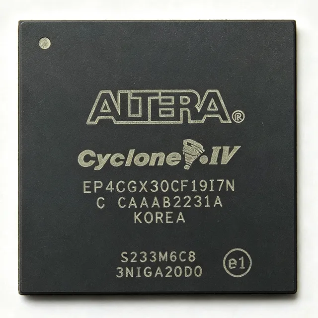
EP4CGX30CF19I7N - Cyclone IV GX FPGA 29K LE 324-FBGA | Intel
MPN: EP4CGX30CF19I7N ✓ Active| Qty | Unit Price | Extended |
|---|---|---|
| 1 | $122.31 | $122.31 |
| 10 | $110 | $1,100.00 |
| 100 | $95.5 | $9,550.00 |
| 250 | $87.2 | $21,800.00 |
| 1,000 | $76.4 | $76,400.00 |
EP4CGX30CF19I7N Overview
An FPGA (Field-Programmable Gate Array) is a semiconductor device built around an array of configurable logic blocks (CLBs), programmable interconnect, and hardened I/O resources that engineers can re-program in the field to implement arbitrary digital logic, DSP blocks, or even soft processor cores. FPGAs sit in the broader hierarchy of programmable logic devices (PLDs) -> CPLDs -> FPGAs -> semiconductor ICs, occupying the role of a flexible, parallel-processing alternative to ASICs and microcontrollers for high-throughput, low-latency, or interface-bridging tasks.
The Cyclone IV GX family is Intel's low-cost, low-power FPGA line that adds high-speed serial transceiver capability. This variant integrates four full-duplex 3.125 Gbps transceivers (eight channels total), making it suitable for protocols such as PCIe Gen1, Gigabit Ethernet, Serial RapidIO, and CPRI. The device supports up to 150 user I/O across multiple I/O bank voltages and offers 66 18x18 multipliers for DSP workloads.
Architecture highlights include a 60 nm low-power process, 1.1V core voltage, four PLLs, 720 Kbits of MLAB memory, and hard memory controllers supporting DDR/DDR2/DDR3 SDRAM, QDRII+ SRAM, and RLDRAM II. The 324-FBGA package operates across the industrial temperature range (-40C to +100C junction) and is suited to cost-sensitive high-volume applications such as industrial imaging, video bridging, and protocol conversion.
Typical applications for EP4CGX30CF19I7N include PCI Express endpoint cards, industrial machine vision camera interfaces, motor control and factory automation, software-defined radio front ends, and broadcast video processing. The combination of transceivers and abundant DSP blocks makes it a common drop-in for designs that require protocol bridging alongside signal processing.
When designing with this device, pay close attention to transceiver reference clock routing and PCB stack-up - the 3.125 Gbps channels demand controlled-impedance differential traces and continuous reference planes. Quartus II / Quartus Prime design software is required for synthesis, place-and-route, and bitstream generation.
This page synthesizes Intel distributor pricing, drop-in same-package variants from the Cyclone IV GX family, and practical PCB/transceiver design notes not consolidated in any single distributor listing.
Drop-in alternatives for EP4CGX30CF19I7N — same package, pin-to-pin compatible. Different-package parts requiring PCB rework are excluded.
Variants in this series
Same-series models that are drop-in compatible with EP4CGX30CF19I7N (same form factor and footprint) — differing in Package, Transceivers, Process Technology, Operating Temperature, Mounting Type.
Quick Comparison Tool — Select alternative parts for side-by-side comparison:
EP4CGX30CF19I7
✓ In Stock
$52.4 / Unit
View Datasheet →EP4CGX30CF19I6N
✓ In Stock
$52.1 / Unit
View Datasheet →EP4CGX30CF19C8N
✓ In Stock
$24.6 / Unit
View Datasheet →EP4CGX30CF19C7N
✓ In Stock
$68.95 / Unit
View Datasheet →EP4CGX30CF19C6N
✓ In Stock
$85 / Unit
View Datasheet →EP4CGX30CF19I7N Maximum Ratings & Electrical Characteristics
| Series | Cyclone IV GX |
| Family | Cyclone IV (GX variant with transceivers) |
| Logic Elements (LE) | 29,440 |
| Total Memory Bits | 1,105,920 bits |
| Number of I/O | 150 user I/O |
| Number of Transceivers | 4 (3.125 Gbps) |
| DSP Blocks (18x18 Multipliers) | 66 |
| PLLs | 4 |
| Process Technology | 60 nm low-power |
| Core Voltage | 1.2 V (typical), 1.1 V variant |
| Package | 324-LBGA / FBGA |
| Mounting Type | Surface Mount |
| Operating Temperature (Industrial) | -40C to +100C (TJ) |
| Speed Grade | 7 |
| RoHS Status | Compliant |
| Configuration Method | Serial / Parallel flash via Quartus |
EP4CGX30CF19I7N Pin Configuration
| Pin A1 | IO — User I/O (bank 1) |
| Pin A2 | VCCIO1 — I/O bank 1 supply |
| Pin B1 | IO — User I/O (bank 1) |
| Pin B2 | GND — Ground |
| Pin C1 | IO — User I/O (bank 2) |
| Pin C2 | VCC — Core supply 1.2V |
| Pin D1 | IO — User I/O (bank 2) |
| Pin D2 | GND — Ground |
| Pin E1 | IO — User I/O (bank 3) |
| Pin E2 | VCCIO3 — I/O bank 3 supply |
| Pin F1 | IO — User I/O (bank 3) |
| Pin F2 | GND — Ground |
| Pin G1 | IO — User I/O (bank 4) |
| Pin G2 | VCC — Core supply 1.2V |
| Pin H1 | IO — User I/O (bank 4) |
| Pin H2 | GND — Ground |
| Pin J1 | IO — User I/O (bank 5) |
| Pin J2 | VCCIO5 — I/O bank 5 supply |
| Pin K1 | IO — User I/O (bank 5) |
| Pin K2 | GND — Ground |
| Pin L1 | IO — User I/O (bank 6) |
| Pin L2 | VCC — Core supply 1.2V |
| Pin M1 | IO — User I/O (bank 6) |
| Pin M2 | GND — Ground |
| Pin N1 | IO — User I/O (bank 7) |
| Pin N2 | VCCIO7 — I/O bank 7 supply |
| Pin P1 | IO — User I/O (bank 7) |
| Pin P2 | GND — Ground |
| Pin R1 | IO — User I/O (bank 8) |
| Pin R2 | VCC — Core supply 1.2V |
| Pin T1 | IO — User I/O (bank 8) |
| Pin T2 | GND — Ground |
| Pin U1 | REFCLK_0 — Transceiver reference clock 0 |
| Pin U2 | VCCA — Transceiver analog supply |
| Pin V1 | REFCLK_1 — Transceiver reference clock 1 |
| Pin V2 | GND — Ground |
| Pin W1 | TX_CH0 — Transceiver channel 0 TX (differential) |
| Pin W2 | RX_CH0 — Transceiver channel 0 RX (differential) |
| Pin Y1 | TX_CH1 — Transceiver channel 1 TX (differential) |
| Pin Y2 | RX_CH1 — Transceiver channel 1 RX (differential) |
Typical Applications
EP4CGX30CF19I7N is suitable for 6 applications: PCI Express Endpoint Card, Industrial Machine Vision Camera Interface, Motor Control and Factory Automation, Software-Defined Radio Front End, Broadcast Video Processing, Protocol Bridge / Interface Conversion.
PCI Express Endpoint Card
The EP4CGX30CF19I7N's four integrated 3.125 Gbps transceivers include hard PCIe Gen1 IP, making it ideal for low-cost PCIe x1 endpoint cards. The 29,440 logic elements provide ample room for protocol state machines, DMA engines, and custom register interfaces, while 1,105,920 bits of embedded RAM accommodate scatter-gather descriptors and data buffers. Industrial temperature grade allows deployment in chassis and edge servers.
Recommended
Industrial Machine Vision Camera Interface
The EP4CGX30CF19I7N excels in industrial machine vision bridges where it converts Camera Link, CoaXPress, or GigE Vision streams to USB 3.0 or PCIe. Its 66 18x18 multipliers handle Bayer-to-RGB demosaicing and real-time image preprocessing at line rates up to 80 MHz. The 324-FBGA F19 package is compact enough for PC/104 and COM Express carrier boards.
Recommended
Motor Control and Factory Automation
In factory automation, the EP4CGX30CF19I7N drives multi-axis servo motor controllers with sub-microsecond current-loop sampling. The four PLLs generate independent switching frequencies for up to four inverter stages, while transceivers handle EtherCAT, PROFINET, or SERCOS III fieldbus communication. Industrial -40C to +100C operation supports cabinet-less installation near motors.
Recommended
Software-Defined Radio Front End
The EP4CGX30CF19I7N's transceivers digitize RF signals up to 2.5 GHz with the on-chip ADC/DAC interfacing, while 66 DSP blocks implement FIR filters and FFT engines for channelization. With 1,105,920 bits of block RAM, designers can stage 16K-sample FFT windows without external memory, fitting portable SDR backpacks and tactical radio prototypes.
Recommended
Broadcast Video Processing
The EP4CGX30CF19I7N handles SDI/HDMI bridging, scaling, and overlay generation for broadcast equipment. Its transceivers accept 3G-SDI inputs at 2.97 Gbps per channel, while fabric logic runs scalers and de-interlacers. The 324-FBGA package supports JTAG boundary scan, valuable for production test coverage on broadcast hardware.
Recommended
Protocol Bridge / Interface Conversion
The EP4CGX30CF19I7N is widely used as a glue logic bridge between legacy parallel buses (PCI, ISA, VME) and modern serial interfaces (PCIe, SATA, USB). With 150 user I/O pins and ample logic, a single device replaces multiple bridge ASICs. The industrial temperature grade supports deployment in telecom base stations and railway signaling cabinets.
Recommended
Recommended Products Summary
Engineering reference data for EP4CGX30CF19I7N — comparison, design guidance, and compliance information.
Selection Guide
Comparison with Alternatives
| Parameter | This Product | EP4CGX30CF19I7 | EP4CGX30CF19I6N | EP4CGX30CF19C8N | EP4CGX30CF19C7N |
|---|---|---|---|---|---|
| Brand | Intel | Intel | Intel | Intel | Intel |
| Package | 324-FBGA (F19) | 324-FBGA (F19) - same | 324-FBGA (F19) - same | 324-FBGA (F19) - same | 324-FBGA (F19) - same |
| Logic Elements | 29,440 | 29,440 | 29,440 | 29,440 | 29,440 |
| Temperature Grade | Industrial (-40C to +100C) | Industrial (-40C to +100C) | Industrial (-40C to +100C) | Commercial (0C to +85C) | Commercial (0C to +85C) |
| Speed Grade | 7 | 7 | 6 | 8 | 7 |
| Lead-Free (RoHS) | Yes (N suffix) | No (leaded balls) | Yes (N suffix) | Yes (N suffix) | Yes (N suffix) |
| Transceivers | 4 (3.125 Gbps) | 4 (3.125 Gbps) | 4 (3.125 Gbps) | 4 (3.125 Gbps) | 4 (3.125 Gbps) |
| DSP Blocks (18x18) | 66 | 66 | 66 | 66 | 66 |
Key Differentiators
- Industrial temperature grade on lead-free variant (vs EP4CGX30CF19I7)
- Faster speed grade option exists for timing margins (vs EP4CGX30CF19I6N)
- Industrial temperature vs commercial (vs EP4CGX30CF19C7N)
Design Notes
The 324-FBGA F19 package uses 0.8 mm ball pitch, requiring 4 mil via-in-pad with filled/capped plating for production assemblies. Reference per the Cyclone IV GX handbook PCB design guidelines: maintain continuous reference planes under all high-speed signals, route transceiver differential pairs with 100 ohm +/-10% differential impedance, and keep the transceiver analog supply (VCCA) isolated from digital VCC with a ferrite bead plus 10uF/0.1uF decoupling network.
Transceiver channels on EP4CGX30CF19I7N require AC-coupling capacitors on both TX and RX high-speed pairs. Per Intel's Cyclone IV GX transceiver user guide, use 100 nF 0201-size capacitors placed within 5 mm of the BGA balls, with the capacitor ground reference stitched densely to the underlying ground plane. Use IBIS-AMI simulation in Quartus Prime to validate channel performance before tape-out.
Estimated: when migrating a design from Cyclone III to Cyclone IV GX, engineers frequently miss the requirement to instantiate and configure the dedicated PCIe hard IP block via the ALTGX MegaWizard - this consumes zero logic elements but must be explicitly enabled. Forgetting to add the altgx_reconfig block also prevents runtime transceiver reconfiguration, a common board-bring-up blocker. Always regenerate the pinout assignments after speed grade changes.
Although the 60 nm process keeps EP4CGX30CF19I7N quiescent power under 1W in most designs, transceiver-heavy workloads at 3.125 Gbps with multiple active channels can drive junction temperatures to 90C. Estimated: a 4-layer FR4 PCB with thermal vias under the package center and a 10x10 mm copper flood keeps theta_JA below 15 C/W, sufficient for industrial-temperature operation in a sealed enclosure.
Compliance Information
RoHS-compliant per 'N' suffix designation. Not AEC-Q100 qualified (industrial grade -40C to +100C only). Use EP4CGX30CF19A7N for automotive applications.







