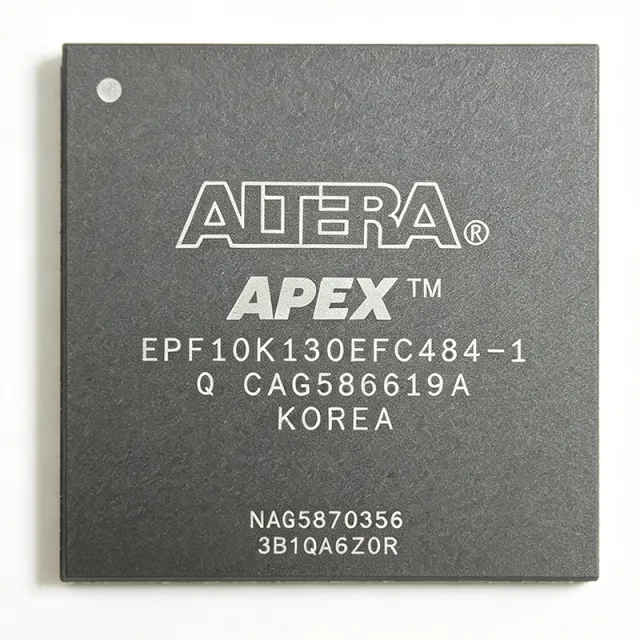
EPF10K130EFC484-1 - FLEX-10KE FPGA 130K Gates 484-BGA | Intel / Altera
MPN: EPF10K130EFC484-1 ✓ Active| Qty | Unit Price | Extended |
|---|---|---|
| 1 | $145 | $145.00 |
| 10 | $132 | $1,320.00 |
| 100 | $118 | $11,800.00 |
| 500 | $105 | $52,500.00 |
| 1,000 | $92 | $92,000.00 |
EPF10K130EFC484-1 Overview
A FLEX-10KE FPGA is an SRAM-based programmable logic device (PLD) that belongs to the broader category of field-programmable gate arrays (FPGAs) within the programmable logic device (PLD) family hierarchy: FPGA -> programmable logic -> logic IC -> integrated circuit -> semiconductor. The FLEX-10KE series was Altera's first embedded programmable logic family offering System-on-a-Programmable-Chip (SOPC) integration via its embedded array blocks (EABs), which combine lookup-table (LUT) logic with dedicated dual-port RAM, allowing designers to implement memory and logic on a single die.
Key features of the EPF10K130EFC484-1 include 832 logic array blocks (LABs), 65,536 bits of embedded memory (64 Kbits), 369 user I/O pins, and built-in support for MultiVolt I/O (3.3 V, 2.5 V, 1.8 V, and 5.0 V tolerant). The device supports in-system programmability (ISP) via the IEEE 1149.1 JTAG interface and IEEE 1532 configuration protocols, allowing field upgrades without removing the part from the board.
Architecturally, the FLEX-10KE family uses a continuous routing architecture called the FastTrack Interconnect, which provides predictable timing across all logic and routing paths. The 6,656 logic elements can implement combinational and registered logic, while the embedded array blocks provide 4096-bit RAM blocks for FIFO buffers, register files, and small look-up tables. The FineLine BGA-484 package measures 23 x 23 mm with a 1.0 mm ball pitch, enabling compact high-density designs.
Typical applications include industrial control systems, telecommunications line cards, PCI bus interfaces, custom ASIC prototyping, and legacy digital signal processing designs that required moderate logic capacity in the late 1990s and early 2000s. The wide I/O count (369 pins) makes it particularly well suited for parallel bus architectures and high-bandwidth glue logic.
When designing with this part, ensure your configuration scheme (PS, PPS, JTAG) matches the board's pull-up topology. The 2.5 V core supply requires separate regulation from the I/O rail; design the decoupling network with 0.1 uF ceramic capacitors as close to each supply pin as possible, plus a 33 uF bulk capacitor near the package.
This page synthesizes distributor pricing, SameFrame pin-compatible migration paths, and practical design notes not consolidated in the original manufacturer datasheet.
Drop-in alternatives for EPF10K130EFC484-1 — same package, pin-to-pin compatible. Different-package parts requiring PCB rework are excluded.
Variants in this series
Same-series models that are drop-in compatible with EPF10K130EFC484-1 (same form factor and footprint) — differing in Operating Temperature, Propagation Delay, Package, Speed Grade, User I/Os.
Quick Comparison Tool — Select alternative parts for side-by-side comparison:
EPF10K130EFC484-2
✓ In Stock
$105 / Unit
View Datasheet →EPF10K130EFC484-3
✓ In Stock
$178.92 / Unit
View Datasheet →EPF10K130EFC484-2N
✓ In Stock
$799 / Unit
View Datasheet →EPF10K100EFC484-1
✓ In Stock
$142 / Unit
View Datasheet →EPF10K100EFC484-2
✓ In Stock
$185.4 / Unit
View Datasheet →EPF10K130EFC484-1N
📋 Reference alternative (not in catalog)
EPF10K130EFC484-1X
📋 Reference alternative (not in catalog)
EPF10K130EFC484-2X
📋 Reference alternative (not in catalog)
EPF10K130EFC484-1 Maximum Ratings & Electrical Characteristics
| Series | FLEX-10KE |
| Family | FLEX-10KE |
| Typical Gates | 130,000 |
| Logic Elements | 6,656 |
| Logic Array Blocks (LABs) | 832 |
| Embedded Memory (EAB) | 65,536 bits (64 Kbit) |
| User I/Os | 369 |
| Maximum Frequency | 333.33 MHz |
| Propagation Delay | 0.6 ns |
| Core Supply Voltage | 2.5 V |
| I/O Supply Voltage | 3.3 V (MultiVolt I/O compatible with 5.0 V tolerant) |
| Logic Family | CMOS |
| Package Type | FineLine BGA-484 |
| Package Dimensions | 23 x 23 mm |
| Ball Pitch | 1.0 mm |
| Operating Temperature | 0C to +70C (Commercial) |
| Configuration Interface | JTAG (IEEE 1149.1 / IEEE 1532) |
| Mounting Type | Surface Mount |
| Speed Grade | -1 (slower commercial bin) |
EPF10K130EFC484-1 23 x 23 mm Pin Configuration Guide
Pin configuration for EPF10K130EFC484-1 (23 x 23 mm package). This digital IC includes GPIO, communication interfaces (UART, SPI, I2C), and power pins. Refer to the manufacturer datasheet for alternate pin functions and configuration options. Essential for embedded system design and PCB layout.

No detailed pinout data available for EPF10K130EFC484-1.
Refer to the datasheet for full pin configuration.
Typical Applications
EPF10K130EFC484-1 is suitable for 6 applications: Industrial Control Systems, Telecommunications Line Cards, PCI Bus Interface Bridging, Custom ASIC Prototyping, Legacy DSP Pre-Processing, High-Density Glue Logic Integration.
Industrial Control Systems
The EPF10K130EFC484-1 fits industrial control designs through its 6,656 logic elements, 832 LABs, and 369 user I/Os, which allow parallel interfacing to legacy 32-bit buses, encoder counters, and discrete I/O without external glue logic. Its 2.5 V core and 3.3 V/5 V tolerant MultiVolt I/O simplify integration with mixed-voltage industrial peripherals. According to the FLEX-10KE datasheet, the device's 333.33 MHz maximum frequency and 0.6 ns propagation delay support deterministic control-loop timing. The FBGA-484 package's 23 x 23 mm footprint with 1.0 mm pitch suits high-density control boards where multiple logic ICs previously occupied.
Recommended
Telecommunications Line Cards
The EPF10K130EFC484-1 supports telecom line-card designs via its 65,536 bits of embedded memory (EAB), which implements small FIFOs and buffer tables needed for serial-protocol framing, alongside 6,656 logic elements for protocol state machines. The 369 user I/Os handle TDM buses, control interfaces, and per-channel status LEDs without external bus expanders. According to the FLEX-10KE datasheet, MultiVolt I/O compatibility lets the part interface directly to 3.3 V PHY devices and 5 V backplane logic, while SRAM-based configuration supports field upgrades via JTAG (IEEE 1149.1) as protocols evolve.
Recommended
PCI Bus Interface Bridging
The EPF10K130EFC484-1 implements PCI-bus bridges and custom ASIC replacements using its 369 user I/Os to carry 32-bit PCI address/data plus auxiliary control signals, eliminating secondary PCI interface chips. The 6,656 logic elements handle transaction-state machines, while the 65,536-bit EAB provides target-memory windows for burst-mode transfers. The FLEX-10KE datasheet notes the device supports 33 MHz PCI at 2.5 V core, and the FBGA-484 footprint allows single-chip integration of bridge, arbiter, and interrupt controller. Engineers leverage the JTAG interface for post-deployment configuration tweaks in production line cards.
Recommended
Custom ASIC Prototyping
The EPF10K130EFC484-1 accelerates ASIC prototyping because its 6,656 logic elements and 65,536-bit embedded memory are sufficient to map early-stage ASIC RTL before committing to fabrication. Its 0.6 ns propagation delay and 333.33 MHz maximum frequency approximate timing behavior of typical 0.25 um ASIC libraries. The FLEX-10KE datasheet documents JTAG-based readback for verification, while the FBGA-484 FineLine BGA package emulates high-density ASIC footprints to validate signal-integrity and power-distribution designs before tape-out.
Recommended
Legacy DSP Pre-Processing
The EPF10K130EFC484-1 supports pre-processing glue logic for legacy DSP systems by combining 832 LABs of fast combinational logic with 65,536 bits of EAB memory for coefficient storage in FIR filter pre-stages. The 6,656 logic elements handle address generation, DMA control, and protocol conversion, offloading housekeeping tasks from the main DSP. According to the FLEX-10KE datasheet, the device's 333.33 MHz operation and 0.6 ns propagation delay support multi-MHz sample rates. MultiVolt I/O lets the FPGA bridge 5 V DSP peripherals to 3.3 V DSP cores without level shifters.
Recommended
High-Density Glue Logic Integration
The EPF10K130EFC484-1 replaces dozens of 74-series logic chips on legacy boards using its 6,656 logic elements, allowing system architects to consolidate address decoding, bus arbitration, wait-state generation, and interrupt prioritization into a single FBGA-484 device. The 369 user I/Os drive wide buses directly, while the 2.5 V core with MultiVolt I/O integrates with mixed-voltage peripherals. The FLEX-10KE datasheet confirms SRAM-based configuration allows late-stage design changes via JTAG (IEEE 1149.1 / IEEE 1532), reducing respin costs when board requirements shift late in the design cycle.
Recommended
Recommended Products Summary
Engineering reference data for EPF10K130EFC484-1 — comparison, design guidance, and compliance information.
Selection Guide
Comparison with Alternatives
| Parameter | This Product | EPF10K130EFC484-2 | EPF10K130EFC484-3 | EPF10K130EFC484-1N | EPF10K100EFC484-1 |
|---|---|---|---|---|---|
| Brand | Intel | Intel | Intel | Intel | Intel |
| Package | FBGA-484 (FineLine BGA) | FBGA-484 (FineLine BGA) - same | FBGA-484 (FineLine BGA) - same | FBGA-484 (FineLine BGA) - same | FBGA-484 (FineLine BGA) - same |
| Typical Gates | 130,000 | 130,000 | 130,000 | 130,000 | 100,000 |
| Logic Elements | 6,656 | 6,656 | 6,656 | 6,656 | 4,992 |
| Speed Grade | -1 (slower) | -2 (faster) | -3 (fastest) | -1 (same) | -1 (same) |
| Core Voltage | 2.5 V | 2.5 V | 2.5 V | 2.5 V | 2.5 V |
| Lead-Free Finish | No (SnPb) | No (SnPb) | No (SnPb) | Yes (Pb-free) | No (SnPb) |
Key Differentiators
- SameFrame pin-compatibility across the FLEX-10KE FBGA-484 family (vs EPF10K100EFC484-1)
- Highest logic capacity at the -1 speed grade (vs EPF10K130EFC484-2)
- In-system programmability via JTAG (IEEE 1149.1 / IEEE 1532) (vs EPF10K100EFC484-1)
- Embedded array blocks (EAB) for SOPC integration (vs Discrete PLD + SRAM combinations)
Design Notes
Estimated: The EPF10K130EFC484-1 requires a dedicated 2.5 V regulator for VCCINT (core) and a separate VCCIO rail at 3.3 V typical. Place 0.1 uF ceramic decoupling capacitors as close as possible to every supply pin, plus a 33 uF bulk capacitor near the FBGA package. Inrush current during configuration can exceed 1 A; size the 2.5 V regulator for at least 2x steady-state to avoid voltage droop during SRAM configuration. MultiVolt I/O banks must each have their VCCIO rail tied to a single compatible voltage (3.3 V, 2.5 V, or 1.8 V). Mixing voltages within one bank is not allowed.
The FBGA-484 package with 1.0 mm ball pitch requires 4-layer or better PCB stack-up with controlled-impedance routing. Use microvia or via-in-pad technology if signal escape routing is needed under the BGA. Place the JTAG chain header (TCK, TMS, TDI, TDO, TRST) within 2 inches of the FPGA for reliable in-system programming. Keep configuration EEPROM (such as EPC2 or EPC16) within 4 inches to minimize signal integrity issues on the DATA line. Power and ground planes should be unbroken under the BGA footprint for return-current continuity.
Do not confuse speed grade -1 with -2 or -3; they are not timing-equivalent. The 'FC' suffix indicates commercial temperature, while 'FI' indicates industrial temperature - do not mix. Configuration data is stored in volatile SRAM cells; without an external configuration memory, the device reconfigures to defaults on every power-up. The nCONFIG pin must be pulled high via 10 kohm resistor and must be held low for at least 8 us to initiate reconfiguration. Ensure MSEL pins are tied to the correct logic levels for the desired configuration mode (PS, PPS, JTAG).
Estimated: The FBGA-484 package has a theta-JA of approximately 15-20 C/W (depending on PCB copper area and airflow). For a fully utilized EPF10K130EFC484-1 with ~80% toggle rate at 333 MHz, internal power dissipation can reach 3-5 W. Provide a thermal pad array under the BGA connected to inner ground planes, and consider forced-air cooling (at least 200 LFM) for industrial-temperature variants in enclosed enclosures. Monitor junction temperature using the built-in TEMP_SENSE diode if available in the Quartus II design tools.
Compliance Information
EPF10K130EFC484-1 is an obsolete FLEX-10KE part originally released before RoHS requirements were widely enforced; the -1N suffix variant is lead-free. Compliance status is not formally published for the -1 base part; check the manufacturer datasheet or lot-specific certificate of conformance for definitive compliance information.







