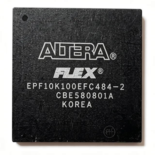
EPF10K100EFC484-1 - FLEX 10KE FPGA 100K Gates 484-BGA | Intel
MPN: EPF10K100EFC484-1 ✓ Active| Qty | Unit Price | Extended |
|---|---|---|
| 1 | $285 | $285.00 |
| 10 | $245 | $2,450.00 |
| 100 | $198 | $19,800.00 |
| 500 | $165 | $82,500.00 |
| 1,000 | $142 | $142,000.00 |
EPF10K100EFC484-1 Overview
An FPGA (Field-Programmable Gate Array) is a semiconductor device built around an array of configurable logic blocks (CLBs), programmable interconnect, and I/O cells that engineers can customize after manufacture using a hardware description language. FPGAs sit between discrete logic ICs and application-specific integrated circuits in the design hierarchy, offering ASIC-like integration with NRE-free, rapid-turnaround programmability. The FLEX 10KE family specifically pioneered embedded System-on-a-Programmable-Chip (SOPC) integration by combining a logic array with embedded array blocks for on-chip memory.
Key features of the EPF10K100EFC484-1 include 624 Logic Array Blocks (LABs), 0.6 ns propagation delay, support for 3.3 V PCI compliance, embedded IEEE Std. 1149.1 JTAG boundary-scan test circuitry, and in-system configurability via serial or parallel EPROM. The 484-FBGA package (23×23 mm) provides a high-density footprint suitable for high-I/O designs while supporting SameFrame pin migration to other FineLine BGA densities in the family. Each LAB contains 8 logic elements (LEs) and local interconnect, enabling efficient state-machine and datapath implementation.
Architecturally, the EPF10K100EFC484-1 uses SRAM-based configuration memory, requiring a configuration EPROM or JTAG download on every power-up. Its Embedded Array Blocks (EABs) deliver 2 Kbits each (12 EABs × 2 Kbit = 24 Kbits, configurable up to 48 Kbits via dual-port mode), supporting FIFO buffers, ROM lookup tables, and arithmetic operations. The device supports multi-volt I/O standards including 3.3 V, 2.5 V, and 1.8 V, with 5 V PCI tolerance. SameFrame pin-out compatibility across the FLEX 10KE BGA family allows design migration without PCB rework when higher- or lower-density members are needed.
Typical applications include telecommunications line cards, networking bridges and routers, industrial control and factory automation, ASIC prototyping, glue logic replacement, and high-speed data acquisition systems. The combination of 338 user I/Os and 49 Kbits of embedded memory suits designs requiring both extensive parallel interfaces and on-chip buffering. Design migration within the FLEX 10KE BGA family is supported by Altera's SameFrame pin-compatibility scheme, enabling scalable platform designs.
When designing with the EPF10K100EFC484-1, ensure the configuration EPROM is correctly sized for the device bitstream, and provide 3.3 V I/O bank power even for designs operating primarily at 2.5 V core. Decoupling requires bulk and high-frequency ceramics placed within 100 mils of each power pin. The 484-BGA requires controlled-impedance escape routing and a minimum 4-layer PCB stack-up with continuous power/ground planes.
This page synthesizes distributor pricing, drop-in same-family alternatives, and practical BGA design notes that complement the manufacturer datasheet for engineers maintaining legacy FLEX 10KE designs.
Drop-in alternatives for EPF10K100EFC484-1 — same package, pin-to-pin compatible. Different-package parts requiring PCB rework are excluded.
Variants in this series
Same-series models that are drop-in compatible with EPF10K100EFC484-1 (same form factor and footprint) — differing in Package, Operating Temperature, Process Technology, Propagation Delay, Mounting Type.
Quick Comparison Tool — Select alternative parts for side-by-side comparison:
EPF10K100EFC484-2
✓ In Stock
$185.4 / Unit
View Datasheet →EPF10K100EFC484-3
✓ In Stock
$65 / Unit
View Datasheet →EPF10K100EFC484-1X
✓ In Stock
$349.57 / Unit
View Datasheet →EPF10K100EFC484-1N
✓ In Stock
$158 / Unit
View Datasheet →EPF10K130EFC484-1
✓ In Stock
$92 / Unit
View Datasheet →EPF10K100EFC484-1DX
📋 Reference alternative (not in catalog)
EPF10K100EFI484-2N
📋 Reference alternative (not in catalog)
EPF10K100EFC484-1 Maximum Ratings & Electrical Characteristics
| Family | FLEX 10KE |
| Logic Elements / Cells | 4,992 |
| Number of LABs/CLBs | 624 |
| Total RAM Bits | 49,152 |
| Embedded Memory (Kbits) | 48 (12 EABs) |
| Number of Block RAM (EABs) | 12 |
| User I/Os | 338 |
| Total Gates | 257,000 typical system gates |
| Operating Supply Voltage (Core) | 2.5 V |
| Operating Supply Voltage Range | 2.375 V to 2.625 V |
| Process Technology | 0.42 µm CMOS |
| Propagation Delay | 0.6 ns |
| Operating Temperature | 0 °C to 70 °C (commercial) |
| Package | 484-FBGA (FineLine BGA, 23×23 mm) |
| Mounting Type | Surface Mount (SMT) |
| Program Memory Type | SRAM (volatile) |
| Configuration Interface | JTAG (IEEE 1149.1), serial/parallel EPROM |
| PCI Support | 3.3 V PCI compliant |
| RoHS Status | Non-compliant (per Arrow listing) |
| Lifecycle Status | Obsolete (EOL) |
EPF10K100EFC484-1 484-fbga (fineline bga, 23×23 mm) Pin Configuration Guide
Pin configuration for EPF10K100EFC484-1 (484-fbga (fineline bga, 23×23 mm) package). This digital IC includes GPIO, communication interfaces (UART, SPI, I2C), and power pins. Refer to the manufacturer datasheet for alternate pin functions and configuration options. Essential for embedded system design and PCB layout.

No detailed pinout data available for EPF10K100EFC484-1.
Refer to the datasheet for full pin configuration.
Typical Applications
EPF10K100EFC484-1 is suitable for 7 applications: Telecommunications Line Cards, Networking Bridges and Routers, Industrial Control and Factory Automation, ASIC Prototyping, High-Speed Data Acquisition, Legacy Telecom Backplane Glue Logic, Glue Logic and Bus Bridge Consolidation.
Telecommunications Line Cards
The EPF10K100EFC484-1 fits telecommunications line-card designs with its 4,992 logic elements and 338 user I/Os, which are sufficient for T1/E1 framers, HDLC controllers, ATM segmentation-and-reassembly engines, and cross-connect switches. Its 12 embedded array blocks provide 49 Kbits of on-chip dual-port RAM for cell buffering and lookup-table-based routing tables, eliminating external FIFOs that consume board area. The 2.5 V core with 3.3 V PCI-compliant I/O supports co-design with standard telecom bus-interface ASICs. SameFrame pin-compatibility with EPF10K130E allows field upgrades to higher density without PCB rework, an advantage for evolving line-card platforms.
Recommended
Networking Bridges and Routers
The EPF10K100EFC484-1 is well matched to custom bridge/router designs where 338 user I/Os support parallel MII/RMII/GMII PHY interfaces, SPI/UART management channels, and PCI host bus connectivity. Its 4,992 logic elements handle packet classification, VLAN tagging, ACL lookups, and QoS scheduling, while 49 Kbits of embedded memory buffers packet headers and route-cache entries. The 3.3 V PCI-compliance simplifies integration with embedded PowerPC or MIPS host processors common in legacy networking platforms. Engineers should target FLEX 10KE EAB dual-port mode for routing-table RAM to maximize throughput.
Recommended
Industrial Control and Factory Automation
Industrial PLC, motion controller, and factory-automation designs benefit from the EPF10K100EFC484-1's high I/O count (338 pins) for parallel encoder, DAC, and opto-isolated interface channels. Its 4,992 logic elements run custom PID controllers, state machines for sequencing, and protocol bridges (Modbus, Profibus, CANopen), while the 12 EABs hold lookup tables for linearization and S-curve profiling. For industrial temperature operation, the EPF10K100EFI484-2N variant in the same 484-FBGA footprint extends the operating range to -40 °C to +85 °C without PCB rework.
Recommended
ASIC Prototyping
Engineers use the EPF10K100EFC484-1 as an ASIC prototyping vehicle because its 257,000 typical system gates closely match mid-range ASIC densities, allowing full-chip emulation of custom logic before tape-out. The 0.6 ns propagation delay enables verification of high-speed paths, while 49 Kbits of embedded memory emulates on-chip SRAMs without consuming LE-based register banks. JTAG-based configuration via ByteBlaster or USB-Blaster supports rapid design-iteration cycles. The 484-FBGA package exposes enough I/Os to map out large ASIC pad rings, and FLEX 10KE SameFrame compatibility allows migration to EPF10K130E or EPF10K250E for higher gate-count prototyping.
Recommended
High-Speed Data Acquisition
The EPF10K100EFC484-1 supports high-speed data-acquisition front-ends where 338 I/Os connect parallel ADC/DAC data buses, and the 12 EABs (49 Kbits) provide dual-port sample buffering for simultaneous acquire-and-process pipelines. Its 4,992 logic elements handle FIR/IIR filtering, FFT preprocessing, and trigger detection, while SRAM-based configuration enables in-the-field firmware updates for evolving DSP algorithms. The 484-FBGA SameFrame compatibility allows migration to the EPF10K130E when channel counts exceed 4,992-LE capacity without PCB rework.
Recommended
Legacy Telecom Backplane Glue Logic
The EPF10K100EFC484-1 consolidates multiple discrete glue-logic ICs on legacy telecom backplanes — replacing 74-series TTL/CMOS bus transceivers, parity generators, and address-decoder PALs — with 4,992 LEs of programmable logic and 338 user I/Os. Its 3.3 V PCI-compliance and 5 V tolerance simplify retrofits into existing 5 V backplane designs. Embedded JTAG (IEEE 1149.1) supports board-level boundary-scan testing in production, replacing bed-of-nails fixtures. The 484-FBGA SameFrame pinout means existing PCB layouts can be re-populated with EPF10K130E or EPF10K250E if additional logic capacity is needed during board refresh programs.
Recommended
Glue Logic and Bus Bridge Consolidation
The EPF10K100EFC484-1 replaces dozens of discrete 74-series logic, FIFOs, and PAL/GAL devices in mixed-bus systems by implementing custom glue logic, address decoding, wait-state generation, and protocol bridging in a single 484-FBGA package. Its 338 user I/Os cover wide parallel buses (e.g., 32-bit data + 24-bit address + control), and the 49 Kbits of embedded RAM serve as on-chip FIFOs or mailbox registers. The 2.5 V core with multi-voltage I/O (3.3 V, 2.5 V, 1.8 V) bridges mixed-voltage domains without external level shifters.
Recommended
Recommended Products Summary
Engineering reference data for EPF10K100EFC484-1 — comparison, design guidance, and compliance information.
Selection Guide
Comparison with Alternatives
| Parameter | This Product | EPF10K100EFC484-2 | EPF10K100EFC484-3 | EPF10K100EFC484-1X | EPF10K100EFI484-2N |
|---|---|---|---|---|---|
| Brand | Intel | Intel | Intel | Intel | Intel |
| Package | 484-FBGA (FineLine BGA, 23×23 mm) | 484-FBGA - same (SameFrame) | 484-FBGA - same (SameFrame) | 484-FBGA - same | 484-FBGA - same |
| Logic Elements | 4,992 | 4,992 | 4,992 | 4,992 | 4,992 |
| Speed Grade | -1 (slowest) | -2 (mid) | -3 (fastest) | -1 (Rochester long-term) | -2 (industrial) |
| Operating Temperature | 0 °C to +70 °C (commercial) | 0 °C to +70 °C | 0 °C to +70 °C | 0 °C to +70 °C | -40 °C to +85 °C (industrial) |
| User I/Os | 338 | 338 | 338 | 338 | 338 |
| Embedded Memory | 49,152 bits (12 EABs) | 49,152 bits | 49,152 bits | 49,152 bits | 49,152 bits |
| Core Voltage | 2.5 V | 2.5 V | 2.5 V | 2.5 V | 2.5 V |
| Lifecycle Status | Obsolete (EOL) | Obsolete (EOL) | Obsolete (EOL) | Obsolete (Rochester long-term support) | Obsolete (aftermarket) |
| RoHS Status | Non-compliant | Non-compliant | Non-compliant | Non-compliant | Non-compliant |
Key Differentiators
- Mid-density FLEX 10KE with high I/O count for telecom/networking (vs EPF10K50EFC484-1)
- SameFrame 484-FBGA pin compatibility across entire FLEX 10KE family (vs EPF10K100BFC484-1 (legacy FLEX 10KB))
- 12 EABs / 49 Kbits embedded SRAM for on-chip buffering (vs EPF10K100EQC240-1 (240-pin QFP same die))
Design Notes
Estimated: BGA escape routing for the 484-FBGA requires a 4-layer minimum PCB stack-up with continuous ground/power planes. Fan-out should use 0.5–0.8 mm-pitch vias-in-pad or dog-bone fan-out depending on PCB fabrication constraints. Place decoupling capacitors (0.1 µF X7R + 10 µF tantalum per power pin pair) within 100 mils of each supply via to suppress transient currents during simultaneous switching. Keep signal traces away from the BGA corner power/ground balls to avoid discontinuities in the reference plane.
The EPF10K100EFC484-1 requires a 2.5 V core supply (2.375 V–2.625 V) plus separate VCCIO banks for 3.3 V, 2.5 V, or 1.8 V I/O operation. All VCC pins must be connected, even unused banks, to prevent floating supply inputs that cause configuration failure. Estimated: a fully-utilized EPF10K100E draws approximately 200–500 mA core current and an additional 50–200 mA per I/O bank depending on toggle frequency; design the power supply with at least 30 % headroom for inrush during configuration.
Do not skip the configuration EPROM — the EPF10K100EFC484-1 uses SRAM-based configuration memory and must be reconfigured at every power-up via JTAG, serial EPROM, or parallel EPROM. The CONF_DONE pin must pull high within the datasheet-specified tCO time after DCLK starts, or configuration will fail. The MSEL0/MSEL1 pins select the configuration mode and must match the chosen EPROM interface; incorrect settings cause configuration time-out and nSTATUS low.
Estimated: at typical utilization (~70 % LEs active, moderate toggle rate), the EPF10K100EFC484-1 dissipates approximately 1–2 W. The 484-FBGA's thermal resistance (θJA) is roughly 15–20 °C/W on a 4-layer JEDEC test board, giving a 15–40 °C junction rise above ambient. Forced airflow is recommended in enclosed chassis; provide a thermal copper pad connected to the central BGA ground balls for improved heat spreading.
Compliance Information
Arrow listing explicitly states 'EU RoHS Not Compliant' for EPF10K100EFC484-1. The -1N suffix variants from secondary channels may offer lead-free factory finishes, but the base EPF10K100EFC484-1 is non-RoHS. AEC-Q100 not applicable (commercial/industrial FPGA, not automotive-qualified).







