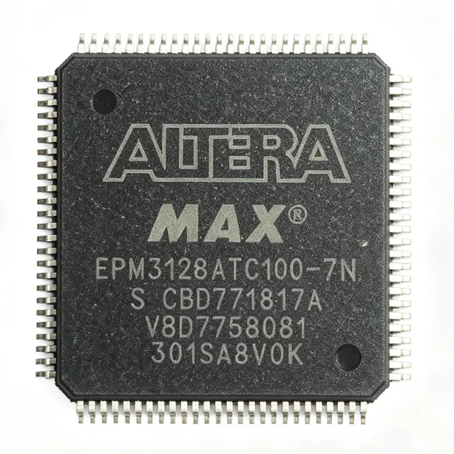
EPM3128ATC100-7N - MAX 3000A 128-Macrocell CPLD, 7.5 ns, TQFP-100 | Intel (Altera)
MPN: EPM3128ATC100-7N ✗ End of Life| Qty | Unit Price | Extended |
|---|---|---|
| 1 | $5.87 | $5.87 |
| 10 | $5.29 | $52.90 |
| 100 | $4.7 | $470.00 |
| 500 | $4.11 | $2,055.00 |
| 1,000 | $3.52 | $3,520.00 |
EPM3128ATC100-7N Overview
A CPLD (Complex Programmable Logic Device) is a non-volatile programmable logic device that combines multiple PAL-like logic blocks with a programmable interconnect matrix, providing deterministic, instant-on glue logic and I/O expansion. Within the programmable-logic taxonomy, CPLDs sit alongside FPGAs as the highest-density members of the programmable-logic hierarchy, but they excel at predictable timing, fast input-to-output propagation, and operation without external configuration memory - features that make them ideal for bus interfacing, address decoding, and control logic.
Key features include 3.3-V core operation with MultiVolt I/O supporting 5.0-V, 3.3-V, and 2.5-V logic levels, in-system programmability (ISP) through the IEEE 1532 / JTAG interface, and a 4.5-ns pin-to-pin delay available on faster speed grades. The device offers four dedicated inputs and a global clear capability, and its non-volatile EEPROM cells retain configuration without a boot PROM.
Architecturally, the EPM3128ATC100-7N implements 128 macrocells organized into Logic Array Blocks (LABs) with a programmable AND/OR array and product-term allocation. The MAX 3000A family shares a common architecture with MAX 7000/7000AE devices, which simplifies design migration through Altera's legacy MAX+PLUS II and Quartus II toolchains.
Typical applications include address decoding and bus interfacing in microcontroller and DSP systems, glue-logic consolidation in industrial controllers, peripheral I/O expansion, and legacy system modernization where instant-on deterministic logic is required. Designers also deploy it in PCI bus interface glue logic, motor-control feedback conditioning, and discrete-logic replacement on legacy boards.
When designing with this device, ensure 3.3-V core supply stability with adequate bulk decoupling near the TQFP-100 power pins. Verify that I/O bank voltage rails match the driven/received logic levels (5.0-V tolerant I/O on a 3.3-V VCCIO is supported, but not vice versa). For new designs, consider MAX II or MAX V devices for lower power and migration continuity.
This page synthesizes distributor pricing, drop-in alternatives from the Site MPN list, and practical design notes not found in the manufacturer datasheet alone, giving procurement and engineering teams a single decision-grade reference.
Drop-in alternatives for EPM3128ATC100-7N — same package, pin-to-pin compatible. Different-package parts requiring PCB rework are excluded.
Variants in this series
Same-series models that are drop-in compatible with EPM3128ATC100-7N (same form factor and footprint) — differing in Package, Operating Temperature, Propagation Delay (tPD), Usable Gates, Configuration Memory.
Quick Comparison Tool — Select alternative parts for side-by-side comparison:
EPM3128ATC100-7
✓ In Stock
$9.2 / Unit
View Datasheet →EPM3128ATC100-5N
✓ In Stock
$8.2 / Unit
View Datasheet →EPM3128ATC100-10N
✓ In Stock
$5.2 / Unit
View Datasheet →EPM3128ATC100-10
✓ In Stock
$8.1 / Unit
View Datasheet →EPM3128ATC100-5
✓ In Stock
$15.43 / Unit
View Datasheet →EPM3128ATC100-7N Maximum Ratings & Electrical Characteristics
| Family | MAX 3000A |
| Macro Cells | 128 |
| Usable Gates | Up to 10,000 |
| Number of I/Os | 80 |
| Propagation Delay (tPD) | 7.5 ns |
| Counter Frequency (max) | 227.3 MHz |
| Supply Voltage - Core | 3.3 V |
| I/O Interface Levels | 5.0 V / 3.3 V / 2.5 V (MultiVolt I/O) |
| In-System Programmability | Yes (IEEE 1532 / JTAG) |
| Program Memory Type | EEPROM (non-volatile) |
| Operating Temperature | 0C to +70C (Commercial) |
| Package | TQFP-100 (100-pin TQFP, fine-line BGA-256 noted in third-party listings) |
| Mounting Type | Surface Mount |
| Logic Family | CMOS |
| Speed Grade | -7 |
EPM3128ATC100-7N tqfp-100 (100-pin tqfp, fine-line bga-256 noted in third-party listings) Pin Configuration Guide
Pin configuration for EPM3128ATC100-7N (tqfp-100 (100-pin tqfp, fine-line bga-256 noted in third-party listings) package). This digital IC includes GPIO, communication interfaces (UART, SPI, I2C), and power pins. Refer to the manufacturer datasheet for alternate pin functions and configuration options. Essential for embedded system design and PCB layout.

No detailed pinout data available for EPM3128ATC100-7N.
Refer to the datasheet for full pin configuration.
Typical Applications
EPM3128ATC100-7N is suitable for 6 applications: Microcontroller Address / Bus Decode, Glue-Logic Consolidation on Legacy Boards, PCI / ISA Peripheral Interface Logic, Industrial Control / PLC I/O Expansion, Motor Control Feedback and PWM Steering, Legacy System Repair / Replacement Stocking.
Microcontroller Address / Bus Decode
The EPM3128ATC100-7N is widely deployed for address decoding, chip-select generation, and bus-interfacing logic between microcontrollers, DSPs, and peripheral banks. With 128 macrocells and 80 user I/Os, it can decode wide address buses and generate timing-controlled chip selects that offload these tasks from the host CPU, freeing it for application code. The 7.5-ns tPD and 227.3-MHz counter frequency keep decode latency well below a single memory-access cycle, while the EEPROM-based non-volatile configuration eliminates boot-PROM complexity - the device is live within microseconds of power-up, which is essential for deterministic startup in industrial and embedded-control systems.
Recommended
Glue-Logic Consolidation on Legacy Boards
Designers use the EPM3128ATC100-7N to replace dozens of 74-series TTL/CMOS discrete logic ICs with a single programmable device, reducing board area, power, and BOM count. Each of its 128 macrocells can implement equivalent sum-of-products logic, and the MAX architecture's product-term allocator automatically shares terms across multiple outputs. The MultiVolt I/O interface (5.0 V / 3.3 V / 2.5 V) lets the EPM3128ATC100-7N sit between legacy 5-V peripherals and modern 3.3-V cores without level shifters. In-system programmability via JTAG (IEEE 1532) enables on-board rework and design-iteration without removing the part, which is invaluable during legacy board bring-up and field upgrades.
Recommended
PCI / ISA Peripheral Interface Logic
The EPM3128ATC100-7N is a recognized solution for PCI and ISA peripheral interface glue logic, generating command, byte-enable, and parity signals to bridge a host bus to peripherals. Its 80 user I/Os comfortably route a full 32-bit PCI data/address bus plus control lines, while the 7.5-ns tPD supports 33-MHz PCI timing budgets (30 ns cycle). MultiVolt I/O allows the CPLD core to run on 3.3 V while directly driving 5-V PCI signals when required. Non-volatile EEPROM configuration means the part is operational immediately after power-up - critical for PCI bus enumeration that expects peripherals to be ready before host firmware scan begins.
Recommended
Industrial Control / PLC I/O Expansion
In industrial controllers and PLCs, the EPM3128ATC100-7N serves as deterministic state-machine glue logic that orchestrates input debouncing, output sequencing, and interlock conditions. The device's deterministic tPD removes any timing jitter that microcontrollers introduce through software loops, and its EEPROM-based instant-on behavior supports fail-safe startup in safety-relevant circuits. With 80 I/Os, the CPLD can manage dozens of optocoupler-isolated inputs and relay-driver outputs while implementing watchdog and fault-handling state machines. The 0C to +70C commercial temperature range suits cabinet-mounted equipment; for extended-temperature environments, MAX II industrial-grade variants are recommended.
Recommended
Motor Control Feedback and PWM Steering
Motor-drive boards use the EPM3128ATC100-7N to handle encoder feedback capture, Hall-sensor decoding, and PWM steering logic between a DSP/MCU controller and the power stage. The CPLD's high counter frequencies (up to 227.3 MHz) allow precise quadrature-encoder counting at high motor RPM, while the deterministic propagation delay enables dead-time insertion and shoot-through protection in three-phase inverter logic. MultiVolt I/O lets the CPLD directly interface 5-V Hall sensors and 3.3-V DSP GPIOs from the same device, removing level shifters from the BOM. With 128 macrocells, it can simultaneously process feedback and generate commutation timing for multi-axis drives.
Recommended
Legacy System Repair / Replacement Stocking
Because the EPM3128ATC100-7N is NRNR (Not Recommended for New Designs) as of 2026-09-12, repair shops and field-service engineers stock the part alongside -5, -7, and -10 speed grades for legacy board repairs. The TQFP-100 fine-line footprint requires careful rework: a hot-air station with appropriate nozzle and pre-heated board is essential to avoid lifted pads on multi-layer boards. Stocking both N and non-N finish variants ensures coverage of boards built under different RoHS regimes, and having the -10 grade available allows substitution on boards whose timing margins are relaxed.
Recommended
Recommended Products Summary
Engineering reference data for EPM3128ATC100-7N — comparison, design guidance, and compliance information.
Selection Guide
Comparison with Alternatives
| Parameter | This Product | EPM3128ATC100-7 | EPM3128ATC100-5N | EPM3128ATC100-10N | EPM3128ATC100-10 | EPM3128ATC100-5 |
|---|---|---|---|---|---|---|
| Brand | Intel (Altera) | Intel (Altera) | Intel (Altera) | Intel (Altera) | Intel (Altera) | Intel (Altera) |
| Package | TQFP-100 | TQFP-100 - same | TQFP-100 - same | TQFP-100 - same | TQFP-100 - same | TQFP-100 - same |
| Family | MAX 3000A | MAX 3000A | MAX 3000A | MAX 3000A | MAX 3000A | MAX 3000A |
| Macro Cells | 128 | 128 | 128 | 128 | 128 | 128 |
| User I/Os | 80 | 80 | 80 | 80 | 80 | 80 |
| Propagation Delay (tPD) | 7.5 ns | 7.5 ns | 4.5 ns (faster) | 10 ns (slower) | 10 ns (slower) | 4.5 ns (faster) |
| Supply Voltage (Core) | 3.3 V | 3.3 V | 3.3 V | 3.3 V | 3.3 V | 3.3 V |
| Lead-Free / RoHS Finish | Yes (N suffix) | No (non-N suffix) | Yes (N suffix) | Yes (N suffix) | No (non-N suffix) | No (non-N suffix) |
| Operating Temperature | 0C to +70C (Commercial) | 0C to +70C | 0C to +70C | 0C to +70C | 0C to +70C | 0C to +70C |
Key Differentiators
- Balanced 7.5-ns speed grade with full MAX 3000A density (vs EPM3128ATC100-10N)
- RoHS-compliant Pb-free terminal finish (N suffix) (vs EPM3128ATC100-7)
- Lower-density alternatives (EPM3064) are NOT drop-in for this part (vs EPM3064ATC100-10N)
Design Notes
Decouple the EPM3128ATC100-7N core VCC (3.3 V) and each VCCIO bank with 100 nF ceramic capacitors placed within 5 mm of the package pin, plus a 10 uF tantalum bulk capacitor per supply rail. The MultiVolt I/O banks may be powered independently of the core, allowing 5.0-V-tolerant I/O operation while the core runs at 3.3 V; route separate VCCIO planes for mixed-voltage systems and stitch ground returns directly under the TQFP-100 thermal pad region.
Estimated: at typical CMOS CPLD core currents under 100 mA across 3.3 V, power dissipation is well below 1 W and the TQFP-100 package requires no special heatsinking. Ensure the surrounding copper pour on inner PCB layers provides a low-impedance thermal path; in enclosed industrial enclosures with ambient temperatures above 60C, derate I/O drive strength in Quartus settings to reduce on-chip dissipation.
Route JTAG signals (TCK, TMS, TDI, TDO) on an inner layer with a ground shield for noise immunity, and place a 10 kohm pull-up on TCK per IEEE 1532 recommendations. Keep the TQFP-100 fine-line-pitch traces (0.5 mm typical) short to avoid signal integrity issues, and use microvia-in-pad construction if BGA fan-out from the same PCB is present. Verify the TCK rise time stays below 50 ns to match the ByteBlaster / USB-Blaster specification.
Do not assume 5.0-V tolerance on every pin: only the MultiVolt I/O banks tolerate 5.0 V inputs; driving 5 V into a VCCIO bank powered at 2.5 V will damage the device. When migrating from a MAX 7000 design, re-validate timing because MAX 3000A uses a different interconnect matrix. Finally, avoid leaving unused macrocell pins floating - configure them as outputs driving low or as inputs with the internal weak pull-up enabled to prevent oscillation.
Compliance Information
N suffix indicates Pb-free/RoHS-compliant terminal finish per Altera naming convention. REACH, halogen-free, and conflict-mineral declarations not located in the verified web data and marked unknown.







