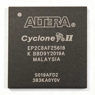
EPM570GF256C4 - MAX II CPLD 570 LE 256-FBGA 5.4ns | Intel
MPN: EPM570GF256C4 ✓ Active| Qty | Unit Price | Extended |
|---|---|---|
| 1 | $45.57 | $45.57 |
| 10 | $41.01 | $410.10 |
| 100 | $36.45 | $3,645.00 |
| 500 | $32.8 | $16,400.00 |
| 1,000 | $29.85 | $29,850.00 |
EPM570GF256C4 Overview
A Complex Programmable Logic Device (CPLD) is a non-volatile, instantly-on programmable logic device that combines multiple PAL/GAL-like logic blocks with a programmable interconnect matrix. Within the broader taxonomy, a CPLD sits between discrete 74-series glue logic (e.g., 74HC, 74LVT) and FPGAs, providing deterministic timing, instant boot-up, and high drive strength for I/O expansion, bus bridging, power sequencing, and interface glue logic. MAX II CPLDs use a flash-based configuration cell, so the device retains its logic image without an external boot PROM and supports in-system programmability via JTAG.
Key features include 5.4 ns tPD (fastest speed grade in the EPM570 family), 8 dedicated input pins, multi-voltage I/O support (1.5 V, 1.8 V, 2.5 V, 3.3 V LVCMOS/LVTTL), 76 to 212 user I/O depending on package, an internal oscillator, and an on-chip voltage regulator that derives the core 1.8 V from an external 2.5 V to 3.3 V VCCINT supply. The 256-ball FBGA provides 212 maximum user I/Os and a 1.0 mm ball pitch.
Architecturally, EPM570GF256C4 partitions its logic into 16 Logic Array Blocks (LABs), each containing 16 Logic Elements with 4-input look-up tables, programmable registers, and a LAB-wide control signal network. The MultiTrack interconnect provides predictable, fixed-delay routing that simplifies static timing closure. JTAG (IEEE 1149.1) is supported for boundary-scan test and in-system programming, and Quartus II (legacy) or Quartus Prime software is used for design entry and device programming.
Typical applications include I/O expansion and voltage translation between 3.3 V MCUs and 1.8 V peripherals, instant-on power sequencing for FPGAs and ASICs, bus interface bridging (e.g., parallel-to-SPI glue), board-level glue logic replacement, and LED/display control in industrial control panels.
When designing with EPM570GF256C4, observe the I/O bank grouping rules in the datasheet: each of the eight I/O banks must be powered by a single VCCIO rail, and unused I/O banks should have their VCCIO tied to a valid voltage to avoid floating inputs. A 100 nF decoupling capacitor should be placed adjacent to every VCCINT/VCCIO pair, and JTAG TCK should be series-terminated when driving long board traces.
This page synthesizes distributor pricing, drop-in alternative MPNs, and practical design notes that complement the manufacturer datasheet.
Drop-in alternatives for EPM570GF256C4 — same package, pin-to-pin compatible. Different-package parts requiring PCB rework are excluded.
Variants in this series
Same-series models that are drop-in compatible with EPM570GF256C4 (same form factor and footprint) — differing in Package, Process Technology, RoHS Status, Operating Temperature, Configuration Memory.
Quick Comparison Tool — Select alternative parts for side-by-side comparison:
EPM570GF256C5
✅ Drop-In✓ In Stock
$18.95 / Unit
View Datasheet →EPM570F256C4N
✅ Drop-In✓ In Stock
$26.85 / Unit
View Datasheet →EPM570GF256C3
✅ Drop-In✓ In Stock
$10.4 / Unit
View Datasheet →EPM570GF256C3N
✅ Drop-In✓ In Stock
$9.4 / Unit
View Datasheet →EPM570F256C5
✅ Drop-In✓ In Stock
$7.1 / Unit
View Datasheet →EPM570GF256C4 Maximum Ratings & Electrical Characteristics
| Family | MAX II |
| Logic Elements (LEs) | 570 |
| Macrocells | 440 |
| Maximum User I/Os | 212 |
| Pin-to-Pin Delay (tPD) | 5.4 ns |
| Supply Voltage VCCINT | 1.71 V to 1.89 V (core, derived from 2.5/3.3 V) |
| I/O Bank Voltage VCCIO | 1.5 V / 1.8 V / 2.5 V / 3.3 V (multi-voltage LVCMOS/LVTTL) |
| Operating Temperature | 0 °C to +85 °C (commercial) |
| Package | 256-ball FBGA (FineLine BGA) |
| Ball Pitch | 1.0 mm |
| Mounting Type | Surface Mount |
| Process Technology | 0.18 µm CMOS, flash-based configuration |
| JTAG Support | IEEE 1149.1 boundary-scan + ISP |
| Configuration Memory | Non-volatile flash (instant-on, no boot PROM) |
| RoHS Status | Lead-free, RoHS compliant |
EPM570GF256C4 256-ball fbga (fineline bga) Pin Configuration Guide
Pin configuration for EPM570GF256C4 (256-ball fbga (fineline bga) package). This digital IC includes GPIO, communication interfaces (UART, SPI, I2C), and power pins. Refer to the manufacturer datasheet for alternate pin functions and configuration options. Essential for embedded system design and PCB layout.

No detailed pinout data available for EPM570GF256C4.
Refer to the datasheet for full pin configuration.
Typical Applications
EPM570GF256C4 is suitable for 6 applications: I/O Expansion and Voltage Translation, Power-Sequencing and Reset Distribution, Bus Bridging and Glue Logic Replacement, Industrial Control Panel Logic, FPGA Configuration and Boot Assistance, LED Display and Signage Control.
I/O Expansion and Voltage Translation
The EPM570GF256C4 is well suited to MCU I/O expansion and voltage translation because it provides up to 212 user I/Os split across 4 to 8 VCCIO banks that can independently run at 1.5 V, 1.8 V, 2.5 V, or 3.3 V. The flash-based, instant-on fabric eliminates external boot PROMs and the deterministic 5.4 ns pin-to-pin delay simplifies timing closure. Typical use: bridge a 1.8 V Cortex-M0+ MCU to legacy 3.3 V peripherals without discrete level-shifters.
Recommended
Power-Sequencing and Reset Distribution
The EPM570GF256C4 is widely used for board-level power sequencing in industrial and telecom hardware where multiple rails must come up in a deterministic order before releasing the host ASIC or FPGA. Its 5.4 ns tPD and 440 macrocells let designers implement multiple independent sequencer state machines with combinational AND/OR glue for fault handling. The flash-based instant-on avoids the boot-PROM delay seen in SRAM FPGAs, ensuring rails are stable within microseconds of VCC ramp.
Recommended
Bus Bridging and Glue Logic Replacement
The EPM570GF256C4 replaces dozens of 74-series glue-logic packages on legacy boards by absorbing address-latch, chip-select, bus-arbiter, and timing-generator functions in a single BGA. With 570 LEs and 440 macrocells, the device can hold multiple parallel-state machines and combinational decoder trees. The JTAG ISP port allows board-level rework without hot-air rework of the BGA, since logic changes are flashed directly into the device.
Recommended
Industrial Control Panel Logic
The EPM570GF256C4's 256-ball FBGA package and multi-voltage I/O make it suitable for industrial control panels where it scans key-matrix inputs, drives 7-segment or LED indicators, and arbitrates between PLC scan cycles and operator pushbuttons. Its 0 to +85 °C commercial temperature range covers most factory-floor enclosures, and the flash configuration retains its logic image across power-cycles for unattended control panels.
Recommended
FPGA Configuration and Boot Assistance
The EPM570GF256C4 is commonly paired with SRAM-based FPGAs to provide the configuration-PROM function, multi-mode boot selection, and partial reconfiguration control. The CPLD's instant-on behavior lets it hold the FPGA in RESET until all rails are stable, then release RESET, drive DONE, and load the bitstream via slave-serial or slave-parallel mode. This pattern is common in Cyclone IV / Cyclone 10 LP reference designs.
Recommended
LED Display and Signage Control
The EPM570GF256C4 drives large LED-matrix displays by generating the row-multiplex timing, PWM dimming waveforms, and refresh-address counters in parallel logic rather than firmware. The 5.4 ns tPD supports high refresh rates with minimal motion-blur, and the 440 macrocells fit multiple PWM channels plus a serial-receive port for incoming video data. Designers typically place the CPLD between a video processor and the LED driver chain.
Recommended
Recommended Products Summary
Engineering reference data for EPM570GF256C4 — comparison, design guidance, and compliance information.
Selection Guide
Comparison with Alternatives
| Parameter | This Product | EPM570GF256C5 | EPM570F256C4N | EPM570GF256C3 | EPM570GF256C3N | EPM570F256C5 |
|---|---|---|---|---|---|---|
| Brand | Intel | Intel | Intel | Intel | Intel | Intel |
| Package | FBGA-256 (1.0 mm pitch) | FBGA-256 (1.0 mm pitch) - same | FBGA-256 (1.0 mm pitch) - same | FBGA-256 (1.0 mm pitch) - same | FBGA-256 (1.0 mm pitch) - same | FBGA-256 (1.0 mm pitch) - same |
| Logic Elements (LEs) | 570 | 570 | 570 | 570 | 570 | 570 |
| Macrocells | 440 | 440 | 440 | 440 | 440 | 440 |
| Pin-to-Pin Delay (tPD) | 5.4 ns | 5.0 ns | 5.4 ns | 6.2 ns | 6.2 ns | 5.0 ns |
| Core Voltage VCCINT | 1.71 V to 1.89 V (from 2.5/3.3 V) | 1.71 V to 1.89 V (from 2.5/3.3 V) | 1.71 V to 1.89 V (from 2.5/3.3 V) | 1.71 V to 1.89 V (from 2.5/3.3 V) | 1.71 V to 1.89 V (from 2.5/3.3 V) | 1.71 V to 1.89 V (from 2.5/3.3 V) |
| Operating Temperature | 0 °C to +85 °C (commercial) | 0 °C to +85 °C | 0 °C to +85 °C | 0 °C to +85 °C | 0 °C to +85 °C | 0 °C to +85 °C |
| RoHS / Lead-Free | Lead-free, RoHS compliant | Lead-free, RoHS compliant | Lead-free, RoHS compliant | Lead-free, RoHS compliant | Lead-free, RoHS compliant | Lead-free, RoHS compliant |
Key Differentiators
- Pin-compatible faster speed grade available for tight timing margins (vs EPM570GF256C5)
- Lead-free variant with identical silicon (vs EPM570F256C4N)
- Multi-voltage I/O banks eliminate external level shifters (vs Discrete 74LVC245 + 74LVC8T245 translators)
Design Notes
Estimated: the EPM570GF256C4 draws approximately 30 to 55 mA quiescent current from VCCINT (2.5 V or 3.3 V) depending on configuration and toggle rate, plus I/O current that scales with VCCIO and switching frequency. Each of the eight VCCIO banks requires a 100 nF decoupling capacitor placed within 3 mm of the ball. Add a bulk 10 µF ceramic or tantalum capacitor on the VCCINT plane and avoid routing high-speed signals across VCCIO bank gaps to maintain signal integrity.
The 256-ball FBGA uses a 1.0 mm pitch, which requires laser-drilled microvias or 0.4 mm via-in-pad technology for reliable fan-out. Recommended stackup is a 4-layer board with continuous GND plane on layer 2 and split VCCINT/VCCIO power planes on layer 3. Keep JTAG TCK/TMS/TDO/TDI traces short and series-terminate TCK at the driver when the trace length exceeds 25 mm to avoid ringing on the boundary-scan clock.
Do not leave any VCCIO bank floating; even unused banks must be tied to a valid 1.5/1.8/2.5/3.3 V rail or the input buffers can draw excess current and produce I/O contention. Avoid mixing LVTTL 3.3 V and LVCMOS 1.8 V on adjacent balls without proper GND via fencing. When migrating from EPM570GF256C4 to EPM570GF256C5 (faster speed grade) re-validate static timing because hold-time violations may appear on short paths that were masked by the slower tPD.
Compliance Information
Lead-free and RoHS compliant per distributor listings. MAX II CPLDs are not AEC-Q100 qualified; for automotive applications a different Intel/Altera CPLD family should be considered.