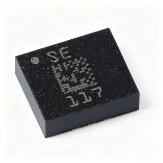
STM32F767VIH6 - 216MHz Cortex-M7 MCU 2MB Flash | ST
MPN: STM32F767VIH6 ✓ Active| Qty | Unit Price | Extended |
|---|---|---|
| 1 | $15.2 | $15.20 |
| 10 | $13.85 | $138.50 |
| 100 | $12.6 | $1,260.00 |
| 500 | $11.4 | $5,700.00 |
| 1,000 | $10.3 | $10,300.00 |
STM32F767VIH6 Overview
A microcontroller (MCU) is a single-chip integrated circuit that combines a processor core, memory, and peripherals into one device, forming the lowest tier of the embedded computing hierarchy: MCU -> embedded processor -> system-on-chip. The STM32F7 series sits at the top of the STM32 general-purpose MCU portfolio, targeting applications that need near-application-processor performance with MCU-class real-time behavior and power consumption.
Key features include the ART Accelerator and 16 Kbyte L1 instruction/data caches enabling 0-wait-state execution from embedded Flash, a single-precision/double-precision FPU and DSP instructions for signal processing, plus rich peripherals including SDRAM interface, TFT LCD controller, hardware JPEG codec, and DFSDM digital filter for sigma-delta modulators.
Architecturally, the Cortex-M7 core pairs with the Chrom-ART Accelerator (DMA2D) for graphics bandwidth offload, while the ART Accelerator prefetches instructions to hide Flash latency at 216 MHz. Multiple embedded SRAM blocks and a flexible external memory controller (FMC) support SDRAM frame buffers for the TFT controller.
Typical applications include industrial HMI and TFT display panels, motor control and power conversion, medical and test equipment, IoT gateways, and consumer devices requiring GUI rendering and fast DSP.
Design consideration: at 216 MHz with external SDRAM, signal integrity and power distribution on the BGA footprint require careful decoupling and length-controlled routing for the FMC interface.
This page synthesizes distributor stock data, drop-in same-family alternatives, and practical design notes not found in the manufacturer datasheet.
Drop-in alternatives for STM32F767VIH6 — same package, pin-to-pin compatible. Different-package parts requiring PCB rework are excluded.
Variants in this series
Same-series models that are drop-in compatible with STM32F767VIH6 (same form factor and footprint) — differing in L1 Cache.
Quick Comparison Tool — Select alternative parts for side-by-side comparison:
STM32F765VIH6
✅ Drop-In✓ In Stock
$9.9 / Unit
View Datasheet →STM32F746VIH6
✅ Drop-In📋 Reference alternative (not in catalog)
STM32F756VIH6
✅ Drop-In ⚠️ 参数待验证📋 Reference alternative (not in catalog)
STM32F767VIH7
✅ Drop-In ⚠️ 参数待验证📋 Reference alternative (not in catalog)
STM32F767VIH6 Maximum Ratings & Electrical Characteristics
| Core | Arm 32-bit Cortex-M7 with DP-FPU |
| Maximum CPU Frequency | 216 MHz |
| Performance | 462 DMIPS / 2.14 DMIPS/MHz |
| Flash Memory | 2 MB (2M x 8) |
| L1 Cache | 16 Kbytes I-cache / D-cache |
| Package | 100-TFBGA (8x8 mm) |
| Mounting Type | Surface Mount |
| Accelerators | ART Accelerator, Chrom-ART (DMA2D) |
| Graphics | TFT LCD controller, hardware JPEG codec |
| External Memory | SDRAM interface via FMC |
| Digital Filter | DFSDM (sigma-delta interface) |
| Instruction Set | Thumb-2, DSP instructions, MPU |
| Series | STM32F7 |
| RoHS Status | Compliant |
| Data Bus Width | 32 bit |
STM32F767VIH6 100-tfbga (8x8 mm) Pin Configuration Guide
Pin configuration for STM32F767VIH6 (100-tfbga (8x8 mm) package). This digital IC includes GPIO, communication interfaces (UART, SPI, I2C), and power pins. Refer to the manufacturer datasheet for alternate pin functions and configuration options. Essential for embedded system design and PCB layout.

No detailed pinout data available for STM32F767VIH6.
Refer to the datasheet for full pin configuration.
Typical Applications
STM32F767VIH6 is suitable for 6 applications: Industrial HMI and TFT Display Panels, Motor Control and Power Conversion, IoT Gateways and Edge Nodes, Medical and Diagnostic Instruments, Audio Processing and DSP, Machine Vision and Camera Interfaces.
Industrial HMI and TFT Display Panels
The STM32F767VIH6 fits industrial human-machine interfaces because its TFT LCD controller, Chrom-ART Accelerator (DMA2D), and hardware JPEG codec offload graphics bandwidth from the 216 MHz Cortex-M7 core, while the FMC SDRAM interface hosts frame buffers externally. Typical usage places the MCU driving an RGB or parallel-interface panel with SDRAM frame buffering, achieving smooth GUI animation without an external graphics processor. The 16 Kbyte L1 caches and ART Accelerator keep GUI code executing at 0 wait states from Flash. The trade-off versus a dedicated SoC is lower peak graphics performance, but significantly lower power, cost, and real-time determinism for control loops running alongside the UI.
Recommended
Motor Control and Power Conversion
For motor drives and digital power, the STM32F767VIH6 combines a 216 MHz Cortex-M7 with DSP instructions and DP-FPU for field-oriented control math, high-resolution timers and ADCs for PWM generation and current sampling, and the DFSDM digital filter for sigma-delta current sensing - a peripheral unique to the F767 tier versus the F765. In practice the MCU executes FOC loops at tens of kilohertz while the caches keep control code deterministic. Using DFSDM with external sigma-delta modulators improves current-sense noise immunity in inverter environments. The consideration is that BGA packages require careful PCB breakout for the dense timer/ADC pin multiplexing, so plan the land pattern fanout early in layout.
Recommended
IoT Gateways and Edge Nodes
The STM32F767VIH6 serves IoT gateways that aggregate sensor data and run protocol stacks: the 2 Mbyte Flash accommodates TLS stacks and firmware-upgrade dual images, the 216 MHz core handles network protocol processing, and DSP instructions accelerate local analytics. Typical designs pair the MCU with Wi-Fi or BLE modules over SPI/UART, storing data in SDRAM or Quad-SPI Flash. The ART Accelerator and L1 caches mitigate Flash latency for compute-heavy preprocessing. Compared with a Linux-class gateway chip, the F767 offers lower power and instant-on real-time response; compared with smaller STM32s, it adds headroom for cryptography and OTA. Choose it when a gateway must also close fast local control loops.
Recommended
Medical and Diagnostic Instruments
Medical monitoring and diagnostic devices benefit from the STM32F767VIH6's combination of DSP capability and the DFSDM digital filter, which accepts external sigma-delta modulators for high-resolution biosignal acquisition (ECG, impedance, audio stethoscope front ends) with excellent noise rejection. The DP-FPU accelerates filtering and analysis algorithms, while 2 Mbytes Flash retains calibration tables and multi-protocol firmware. The TFT controller enables integrated patient-facing displays. In a typical signal chain, modulator clocks derive from the MCU and DFSDM decimates data under DMA, leaving the CPU free for algorithm processing. Note that medical designs must validate the extended temperature grade (STM32F767VIH7) if sterilization or wide ambient range is required.
Recommended
Audio Processing and DSP
The STM32F767VIH6 is well suited to professional audio and active-speaker processing: the 216 MHz Cortex-M7 with DSP instructions executes multiband EQ, dynamic range control, and sample-rate conversion in real time, while SAI/I2S interfaces connect audio codecs and DFSDM accepts digital microphones directly. The DP-FPU provides headroom for 64-bit fixed/float mixing engines, and 2 Mbytes Flash stores DSP libraries plus user presets. A typical topology streams I2S audio under DMA into ping-pong buffers, processes them in cached SRAM for zero-wait-state access, and outputs via SAI. The SDRAM interface supports delay/reverb buffers that exceed on-chip RAM. Versus a dedicated DSP chip, the F767 integrates control and audio in one MCU.
Recommended
Machine Vision and Camera Interfaces
The STM32F767VIH6 supports compact vision nodes through its DCMI camera interface, JPEG codec for on-the-fly image compression, and SDRAM interface for line buffers, reducing bandwidth demands for transmission or storage. The 216 MHz Cortex-M7 with DSP instructions and caches runs classical image preprocessing (histogram, convolution, thresholding) at useful frame rates for QVGA-to-VGA sensors. A typical pipeline captures via DCMI under DMA, compresses to JPEG in hardware, and ships frames over Ethernet-class or serial links. The trade-off versus an ISP-SoC is the absence of an integrated image signal processor, so exposure and simple corrections are handled in firmware; for heavier inference, pair with an AI accelerator module on the same board.
Recommended
Recommended Products Summary
Engineering reference data for STM32F767VIH6 — comparison, design guidance, and compliance information.
Selection Guide
Comparison with Alternatives
| Parameter | This Product | STM32F765VIH6 | STM32F746VIH6 | STM32F756VIH6 | STM32F767VIH7 |
|---|---|---|---|---|---|
| Package | 100-TFBGA (8x8) | 100-TFBGA (8x8) - same | 100-TFBGA (8x8) - same | 100-TFBGA (8x8) - same | 100-TFBGA (8x8) - same |
| Brand | STMicroelectronics | STMicroelectronics | STMicroelectronics | STMicroelectronics | STMicroelectronics |
| Core | Arm Cortex-M7 with DP-FPU | Arm Cortex-M7 with DP-FPU | Arm Cortex-M7 with DP-FPU | Arm Cortex-M7 with DP-FPU | Arm Cortex-M7 with DP-FPU |
| Max CPU Frequency | 216 MHz | 216 MHz | 216 MHz | 216 MHz | 216 MHz |
| Flash Memory | 2 MB | 2 MB | 1 MB | 1 MB | 2 MB |
| TFT LCD Controller | Yes | No | Yes | Yes | Yes |
| JPEG Codec | Yes | No | Yes | Yes | Yes |
Key Differentiators
- Full F767 peripheral set (TFT, JPEG, DFSDM) in TFBGA100 (vs STM32F765VIH6)
- Double the Flash of same-footprint F746/F756 (vs STM32F746VIH6)
- Extended temperature option in same package (vs STM32F767VIH7)
Design Notes
The 8x8 mm TFBGA100 footprint with 0.8 mm ball pitch requires careful fanout planning before routing. Escape via-in-pad or dog-bone escapes are typically needed for dense peripheral multiplexing. Decouple each VDD ball with 100 nF close to the ball, and add bulk 4.7-10 uF per supply domain. Plan the FMC/SDRAM interface first - its clock and data groups benefit from length-matched routing on outer layers with a solid reference plane beneath.
The STM32F767 family supports independent supply domains (VDD, VCAP core regulation, VDDA analog, VBAT backup). Follow the ST reference design: VCAP capacitors per datasheet values are mandatory for internal core regulation stability. Estimated: at 216 MHz running from Flash with peripherals active, core current is typically in the tens of mA range - verify against the datasheet current-consumption tables for your exact peripheral mix before sizing the regulator.
When interfacing SDRAM via FMC at maximum clock rates, keep traces under ~50 mm where possible, series-terminate the clock, and route on a layer adjacent to an unbroken ground plane. On the BGA breakout, avoid stubs on byte-lane signals. ST application notes on FMC/SDRAM interface design provide reference topologies; simulate if your stackup departs from the reference.
Compliance Information
RoHS compliant per ST standard STM32 product pages (ECOPACK). Obtain specific REACH/halogen declarations for this ordering code from st.com.