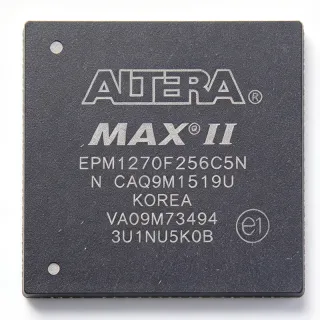
EP2C8F256CXN - Cyclone II FPGA, 8K LEs, 256-FBGA | Altera
MPN: EP2C8F256CXN ✗ End of Life| Qty | Unit Price | Extended |
|---|---|---|
| 1 | $24.5 | $24.50 |
| 10 | $22.1 | $221.00 |
| 100 | $19.75 | $1,975.00 |
| 500 | $17.4 | $8,700.00 |
| 1,000 | $15.2 | $15,200.00 |
EP2C8F256CXN Overview
A Field-Programmable Gate Array (FPGA) is a programmable logic IC containing an array of configurable logic blocks (CLBs), programmable interconnect, and I/O cells, all fabricated on a single silicon die. FPGAs occupy a position in the broader hierarchy of digital semiconductors: programmable logic > logic ICs > integrated circuits > semiconductors. They are typically deployed as glue logic, signal-processing engines, or prototyping platforms where ASIC NRE costs cannot be justified.
Key features include 18 embedded 18x18 multipliers, two PLLs for clock management, and configuration support via active serial (AS), passive serial (PS), and JTAG modes. The device operates from a 1.15 V to 1.25 V core supply with separate VCCIO banks for I/O standard flexibility. The 256-FBGA package offers a compact footprint suitable for space-constrained designs while maintaining sufficient pin count for high-I/O applications.
The Cyclone II architecture is built on SRAM-based configuration memory, requiring an external configuration device for standalone operation. The device family is positioned as a low-cost, low-power alternative to ASICs in volume production for applications such as industrial control, video processing, and communications infrastructure.
Typical applications include motor control, video bridging, industrial Ethernet gateways, and educational/hobbyist development. The 182 user I/O count makes it well-suited for designs that aggregate multiple peripheral interfaces (UART, SPI, I2C, parallel buses) onto a single programmable device.
When designing with this FPGA, ensure the configuration scheme is selected based on the number of devices on the JTAG chain and whether in-system programmability is required. The 256-FBGA package requires careful PCB layout with appropriate via-in-pad or microvia technology to avoid solder joint defects during reflow.
This page synthesizes distributor stock levels, parametric drop-in alternatives from the same Cyclone II family, and PCB layout guidance not typically consolidated on a single manufacturer product page.
Drop-in alternatives for EP2C8F256CXN — same package, pin-to-pin compatible. Different-package parts requiring PCB rework are excluded.
Variants in this series
Same-series models that are drop-in compatible with EP2C8F256CXN (same form factor and footprint) — differing in Package, RoHS Status, Process Technology, Speed Grade, Mounting Type.
Quick Comparison Tool — Select alternative parts for side-by-side comparison:
EP2C8F256C8N
✅ Drop-In✓ In Stock
Contact for price
View Datasheet →EP2C8F256C7N
✅ Drop-In✓ In Stock
$8.31 / Unit
View Datasheet →EP2C8F256C6N
✅ Drop-In✓ In Stock
$31.2 / Unit
View Datasheet →EP2C8AF256A7N
✅ Drop-In✓ In Stock
$41.5 / Unit
View Datasheet →EP2C8AF256I8N
✅ Drop-In✓ In Stock
$21.4 / Unit
View Datasheet →EP2C8F256CXN Maximum Ratings & Electrical Characteristics
| Series | Cyclone II |
| Logic Elements (LEs) | 8,256 |
| Total RAM Bits | 165,888 |
| Embedded 18x18 Multipliers | 18 |
| User I/O Count | 182 |
| PLLs | 2 |
| Core Voltage (VCCINT) | 1.15 V to 1.25 V |
| Operating Temperature | 0C to +85C (commercial) |
| Package | 256-FBGA |
| Mounting Type | Surface Mount |
| Configuration Mode | AS / PS / JTAG |
| Process Technology | 90 nm SRAM |
| RoHS Status | Compliant |
EP2C8F256CXN 256-fbga Pin Configuration Guide
Pin configuration for EP2C8F256CXN (256-fbga package). This digital IC includes GPIO, communication interfaces (UART, SPI, I2C), and power pins. Refer to the manufacturer datasheet for alternate pin functions and configuration options. Essential for embedded system design and PCB layout.

No detailed pinout data available for EP2C8F256CXN.
Refer to the datasheet for full pin configuration.
Typical Applications
EP2C8F256CXN is suitable for 6 applications: Industrial Motor Control, Video Format Conversion / Bridging, Industrial Ethernet Gateway, Digital Signal Processing Front-End, Educational / Hobbyist Development Platform, Legacy Peripheral Aggregation / Glue Logic.
Industrial Motor Control
The EP2C8F256CXN fits industrial motor-control designs where the 8,256 logic elements and 18 dedicated 18x18 multipliers can implement field-oriented control (FOC) algorithms, PWM generation, and encoder decoding in a single chip. Its 182 user I/Os comfortably accommodate multi-axis quadrature encoder inputs, Hall-sensor feedback, and gate-driver interfaces, while the two PLLs provide the deterministic clock synthesis required for high-resolution PWM at 50-100 kHz switching frequencies. The commercial-grade 0C to +85C operating range suits factory-floor control cabinets; choose EP2C8AF256I8N when wider temperature is needed.
Recommended
Video Format Conversion / Bridging
The EP2C8F256CXN is well suited to video bridging applications that convert between parallel RGB, BT.656, BT.1120, and HDMI-style TMDS interfaces. The 165,888 bits of embedded RAM (organized as M9K blocks) buffer scan-line data efficiently, while the 18 hardware multipliers accelerate chroma resampling and scaling arithmetic. With 182 user I/Os and LVDS support, the 256-FBGA package can drive multi-lane flat-panel interfaces directly without external serializer chips, reducing BOM cost in consumer A/V equipment.
Recommended
Industrial Ethernet Gateway
The EP2C8F256CXN supports industrial Ethernet protocols such as PROFINET, EtherCAT, and Modbus TCP by implementing the protocol stack in soft logic alongside a hard Ethernet PHY. The 8,256 LEs are sufficient for medium-complexity MAC implementations and TCP/IP offload, while the 18 hardware multipliers handle wire-speed CRC computation and encryption accelerators. The 256-FBGA package and commercial temperature grade suit DIN-rail-mounted industrial gateways; the embedded PLLs synchronize PHY reference clocks and PTP timestamps.
Recommended
Digital Signal Processing Front-End
The EP2C8F256CXN handles modest DSP workloads such as FIR filtering, FFT pre-processing, and digital down-conversion through its 18 dedicated 18x18 multipliers running at up to ~250 MHz. The 165,888 bits of embedded RAM (M9K blocks) hold coefficients and circular sample buffers, allowing real-time filtering of multi-MHz-bandwidth signals. With 182 user I/Os the device can ingest parallel ADC data at LVDS rates and emit processed streams to downstream DSPs or DACs in instrumentation and SDR front-ends.
Recommended
Educational / Hobbyist Development Platform
The EP2C8F256CXN and its commercial-temperature siblings are widely adopted in university digital-logic courses and hobbyist projects because the Quartus II Web Edition toolchain is free and the device offers a meaningful 8K-LE capacity for teaching Verilog/VHDL, state machines, and embedded soft-core processors. With 182 user I/Os, students can wire up to 7-segment displays, switches, character LCDs, and parallel buses on a single dev board. The 256-FBGA package and abundant I/O flexibility support FPGA-based soft-core CPU labs (Nios II, RISC-V).
Recommended
Legacy Peripheral Aggregation / Glue Logic
The EP2C8F256CXN is frequently deployed as a programmable bridge in legacy industrial systems where it consolidates UART, SPI, I2C, parallel GPIO, and custom timing logic onto a single 182-I/O device. Replacing dozens of 74-series TTL chips, the Cyclone II's 8,256 LEs implement address decoding, bus arbitration, and protocol conversion while the 165 Kbits of embedded RAM support FIFOs and lookup tables. The 256-FBGA package provides a small footprint compared to the equivalent discrete-logic board area, making it ideal for form-factor-constrained retrofits.
Recommended
Recommended Products Summary
Engineering reference data for EP2C8F256CXN — comparison, design guidance, and compliance information.
Selection Guide
Comparison with Alternatives
| Parameter | This Product | EP2C8F256C8N | EP2C8F256C7N | EP2C8AF256I8N |
|---|---|---|---|---|
| Package | 256-FBGA | 256-FBGA - same | 256-FBGA - same | 256-FBGA - same |
| Brand | Altera | Altera | Altera | Altera |
| Logic Elements | 8,256 | 8,256 | 8,256 | 8,256 |
| Total RAM Bits | 165,888 | 165,888 | 165,888 | 165,888 |
| User I/O | 182 | 182 | 182 | 182 |
| Embedded 18x18 Multipliers | 18 | 18 | 18 | 18 |
| PLLs | 2 | 2 | 2 | 2 |
| Speed Grade | Industrial | -8 (fastest) | -7 | -8 industrial temperature |
| Operating Temperature | 0C to +85C (commercial) | 0C to +85C | 0C to +85C | -40C to +100C |
| Lifecycle Status | NRND | NRND | NRND | NRND |
Key Differentiators
- Industrial temperature-grade Cyclone II option with same exact bitstream (vs EP2C8F256C8N)
- Higher logic density than Cyclone II 5K-LE siblings in same package (vs EP2C5F256C8N)
- Bitstream-compatible with all EP2C8F256-family FPGAs (vs EP2C8AF256I8N)
Design Notes
The 256-ball FBGA package on the EP2C8F256CXN requires either microvia (laser-drilled) or via-in-pad PCB technology for reliable solder joint formation during reflow. According to the Cyclone II handbook, the BGA ball pitch is 1.0 mm; designers should use ENIG or OSP surface finish, ensure 4-6 mil trace/space rules, and place decoupling capacitors (0.1 uF and 10 uF) within 100 mils of every VCCINT/VCCIO pin. Thermal vias under the central BGA balls help dissipate the ~1-2 W typical operating power.
The EP2C8F256CXN requires three independent supply rails: VCCINT (1.15-1.25 V, up to ~500 mA), VCCIO (1.5/1.8/2.5/3.3 V per bank, up to ~200 mA per bank), and VCCA_PLL (1.2 V for PLL analog). Per the Cyclone II handbook, all three rails must ramp monotonically and reach stable regulation within 100 ms of each other to avoid configuration errors. A common failure mode is powering VCCIO before VCCINT, which can trigger latch-up on the I/O drivers - sequence VCCINT first, then VCCIO.
Do not attempt to substitute a Cyclone IV (e.g. EP4CE8F256C8N) for the EP2C8F256CXN without recompiling in Quartus. According to Intel's migration document, Cyclone IV uses a different bitstream format and requires re-synthesis, re-fitting, and timing closure - it is NOT a drop-in replacement despite the similar ball-map. For new designs, start with Cyclone IV; for legacy Cyclone II production, stick within the same family (EP2C8F256C8N is the closest speed-grade drop-in).
JTAG chain layout must include the TCK pull-down and TMS pull-up resistors (4.7 kohm typical) recommended by IEEE 1149.1. Per the Cyclone II handbook, JTAG signals should be length-matched within 1 inch and isolated from switching power and clock traces with a ground guard to prevent programming failures. The MSEL[3..0] pins must be tied to fixed logic levels (typically via 4.7 kohm pull-ups to VCCIO) to select active serial vs JTAG configuration at power-up.
Compliance Information
RoHS and lead-free per Altera/Intel PSG product page. Not AEC-Q100 qualified - choose EP2C8AF256I8N for near-automotive. Lifecycle is NRND (Not Recommended for New Designs) - last-ship dates and contractual support continue per Intel PSG FPGA product longevity program.