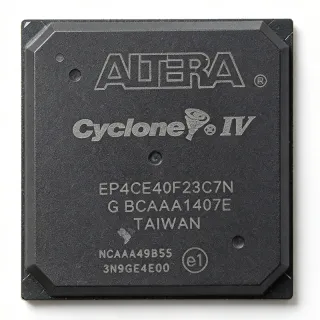
EP2C50F484C8N - Cyclone II FPGA, 50K LE, 484-FBGA | Intel / Altera
MPN: EP2C50F484C8N ⚠ Last Time Buy| Qty | Unit Price | Extended |
|---|---|---|
| 1 | $95 | $95.00 |
| 10 | $88.5 | $885.00 |
| 100 | $78 | $7,800.00 |
| 500 | $72.4 | $36,200.00 |
| 1,000 | $68.2 | $68,200.00 |
EP2C50F484C8N Overview
An FPGA (Field-Programmable Gate Array) is a semiconductor device containing an array of configurable logic blocks (CLBs), programmable interconnects, and dedicated hard IP such as multipliers, memory blocks, and I/O serializers. FPGAs occupy a unique position in the design hierarchy between discrete logic and ASICs: like microcontrollers they are software-programmable, but like ASICs they implement custom parallel hardware. They belong to the broader category of programmable logic devices (PLDs) and are widely used for digital signal processing, protocol bridging, and glue logic in industrial, communications, and consumer systems.
Key features of the EP2C50F484C8N include 50,528 logic elements arranged in LABs (Logic Array Blocks), 250 M4K embedded memory blocks providing 594,432 RAM bits, 86 dedicated 18x18 hardware multipliers, four phase-locked loops (PLLs) for clock management, and 294 user I/Os supporting multiple I/O standards including LVDS, LVTTL, LVCMOS, SSTL, and HSTL. The device operates from a 1.2 V core supply with separate VCCIO banks for I/O voltage flexibility.
The Cyclone II architecture uses SRAM-based configuration memory loaded from a flash or external controller via JTAG or Active Serial (AS) modes. The 484-pin FBGA provides high pin density for designs that need to bring out many parallel interfaces, DDR memory controllers, or multiple high-speed serial channels implemented in LVDS pairs.
Typical applications include industrial motor control, video processing and display controllers, automotive infotainment prototypes, telecommunications line cards, and low-cost digital signal processing (DSP) pipelines. The combination of hardware multipliers, distributed memory, and plentiful I/Os makes this device especially attractive for cost-sensitive DSP and parallel-processing tasks.
When designing with the EP2C50F484C8N, pay attention to power supply sequencing (1.2 V core before VCCIO), decoupling capacitor density near each power pin, and JTAG chain integrity for in-system programming. The FBGA package requires careful PCB layout with microvia technology or proper escape routing.
This page synthesizes distributor pricing, drop-in same-package alternatives, and practical design notes that go beyond the manufacturer datasheet - giving procurement, hardware, and firmware engineers a single reference for sourcing and substituting the EP2C50F484C8N.
Drop-in alternatives for EP2C50F484C8N — same package, pin-to-pin compatible. Different-package parts requiring PCB rework are excluded.
Variants in this series
Same-series models that are drop-in compatible with EP2C50F484C8N (same form factor and footprint) — differing in Package, Speed Grade, Operating Temperature, Process Technology, Configuration Modes.
Quick Comparison Tool — Select alternative parts for side-by-side comparison:
EP2C50F484C7N
✅ Drop-In✓ In Stock
$155 / Unit
View Datasheet →EP2C50F484C6N
✅ Drop-In✓ In Stock
$180.47 / Unit
View Datasheet →EP2C50F484C7
✅ Drop-In✓ In Stock
$165 / Unit
View Datasheet →EP2C50F484C6
✅ Drop-In✓ In Stock
$110 / Unit
View Datasheet →EP2C50F484C8
✅ Drop-In✓ In Stock
$55.4 / Unit
View Datasheet →EP2C50F484C8N Maximum Ratings & Electrical Characteristics
| Family | Cyclone II |
| Series | EP2C50 |
| Logic Elements | 50,528 |
| Total RAM Bits | 594,432 |
| Embedded Memory | 250 M4K blocks |
| User I/Os | 294 |
| 18x18 Hardware Multipliers | 86 |
| PLLs | 4 |
| Speed Grade | -8 (commercial, fast) |
| Package | 484-ball FineLine BGA (FBGA) |
| Mounting Type | Surface Mount (BGA) |
| Core Voltage | 1.2 V |
| I/O Voltage Banks | VCCIO programmable 1.5V/1.8V/2.5V/3.3V |
| Operating Temperature | 0C to +85C (commercial, 'C' suffix) |
| Process Node | 90 nm |
| Configuration Mode | JTAG / Active Serial (AS) |
| RoHS Status | Compliant |
| MSL Level | 3 (168 hours) |
EP2C50F484C8N 484-ball fineline bga (fbga) Pin Configuration Guide
Pin configuration for EP2C50F484C8N (484-ball fineline bga (fbga) package). This digital IC includes GPIO, communication interfaces (UART, SPI, I2C), and power pins. Refer to the manufacturer datasheet for alternate pin functions and configuration options. Essential for embedded system design and PCB layout.

No detailed pinout data available for EP2C50F484C8N.
Refer to the datasheet for full pin configuration.
Typical Applications
EP2C50F484C8N is suitable for 6 applications: Industrial Motor Control, Video Processing and Display Controllers, Telecommunications Line Cards, Automotive Infotainment Prototypes, Low-Cost DSP Pipelines, Custom Protocol Bridging and Glue Logic.
Industrial Motor Control
The EP2C50F484C8N fits industrial motor control applications because its 50,528 logic elements easily host multiple PID control loops, SVPWM modulators, and encoder interfaces in parallel. The 86 dedicated 18x18 hardware multipliers handle Clarke/Park conversions and field-oriented control math without consuming LE resources, while 4 PLLs generate the precisely phase-shifted clocks required for three-phase inverter timing. The 294 user I/Os accommodate multiple Hall sensors, QEP decoders, and gate-driver interfaces in the 484-FBGA package, providing enough headroom for a complete multi-axis controller on a single chip.
Recommended
Video Processing and Display Controllers
The EP2C50F484C8N's 594 Kbits of embedded RAM buffer video line-by-line for deinterlacing, scaling, and color-space conversion in cost-sensitive display applications. The 86 hardware multipliers accelerate 2D FIR filters and chroma upsampling in real time at 60 Hz, while the 294 I/Os simultaneously drive 24-bit RGB panels, BT.656 inputs, and HDMI/DVI bridges via LVDS pairs. The 484-FBGA package escape provides the routing density needed for wide parallel video buses without compromising signal integrity on matched-length traces.
Recommended
Telecommunications Line Cards
The EP2C50F484C8N is well-suited for telecom line-card glue logic and protocol conversion where its 50K logic elements aggregate TDM/E1 streams, perform framing/deframing, and bridge between legacy parallel buses and serial backplanes. Four PLLs provide the multiple clock domains required for TDM, Ethernet, and backplane SERDES references, while the 294 I/Os can interface to multiple framer ICs and T1/E1 transceivers simultaneously. The 484-FBGA footprint supports the dense BGA escape required for cards with high connector pin density.
Recommended
Automotive Infotainment Prototypes
In automotive infotainment prototypes, the EP2C50F484C8N's 50K logic elements implement CAN/LIN gateway logic, audio routing matrices, and HMI controllers before committing to an ASIC. The 86 hardware multipliers accelerate audio DSP for echo cancellation and equalization, while the 294 I/Os accommodate multiple CAN transceivers, LVDS display links, and I2S audio buses. Note that commercial temperature grade (0C to +85C) is sufficient for cabin environments but not under-hood applications, where the EP2C50F484I8N industrial variant is required.
Recommended
Low-Cost DSP Pipelines
The EP2C50F484C8N excels at low-cost DSP pipelines where its 86 dedicated 18x18 hardware multipliers implement FFT, FIR, and IIR filters at hundreds of MSPS without consuming logic elements. The 594 Kbits of M4K RAM block memory provides sample buffering and twiddle-factor storage for streaming DSP, while 50K logic elements handle the control logic, address generation, and ping-pong buffer management. For radar, sonar, vibration analysis, or software-defined radio baseband, this device delivers ASIC-like throughput at FPGA-like NRE economics.
Recommended
Custom Protocol Bridging and Glue Logic
The EP2C50F484C8N provides abundant logic and I/O resources for protocol bridging between SPI, I2C, UART, parallel buses, and custom interfaces in industrial controllers. The 294 user I/Os aggregate dozens of peripheral chips while the 50K logic elements implement state machines, FIFOs, and timing-critical handshaking. Four PLLs derive precise clock domains for each peripheral bus, and the 484-FBGA package supports the wide bus escape required for 16/32-bit parallel memory and peripheral multiplexing.
Recommended
Recommended Products Summary
Engineering reference data for EP2C50F484C8N — comparison, design guidance, and compliance information.
Selection Guide
Comparison with Alternatives
| Parameter | This Product | EP2C50F484C7N | EP2C50F484C6N | EP2C50F484C7 | EP2C50F484C6 | EP2C50F484C8 |
|---|---|---|---|---|---|---|
| Brand | Intel | Intel | Intel | Intel | Intel | Intel |
| Package | 484-FBGA | 484-FBGA - same | 484-FBGA - same | 484-FBGA - same | 484-FBGA - same | 484-FBGA - same |
| Logic Elements | 50,528 | 50,528 | 50,528 | 50,528 | 50,528 | 50,528 |
| Speed Grade | -8 (fastest commercial) | -7 (~10% slower) | -6 (~15% slower) | -7 (~10% slower) | -6 (~15% slower) | -8 (same) |
| User I/Os | 294 | 294 | 294 | 294 | 294 | 294 |
| Embedded RAM | 594,432 bits | 594,432 bits | 594,432 bits | 594,432 bits | 594,432 bits | 594,432 bits |
| Hardware Multipliers (18x18) | 86 | 86 | 86 | 86 | 86 | 86 |
| Temperature Grade | Commercial (0C to +85C) | Commercial | Commercial | Commercial | Commercial | Commercial |
Key Differentiators
- Highest speed grade in the Cyclone II family for commercial temperature (vs EP2C50F484C7N)
- Largest Cyclone II density in 484-FBGA package (vs EP2C35F484C8N)
- RoHS-compliant Pb-free terminal finish (vs EP2C50F484C8 (non-N variant ordering code))
Design Notes
The EP2C50F484C8N requires careful power sequencing: the 1.2 V VCCINT core supply must ramp before or simultaneously with the VCCIO bank supplies to avoid latch-up. Use a supervisor IC or MOSFET-based sequencer to enforce this order. Decoupling requires at least one 0.1 uF MLCC per power pin plus bulk 47 uF tantalum or polymer capacitors on each supply rail, placed within 100 mils of the BGA balls.
The 484-FBGA package demands microvia or via-in-pad technology for clean power and ground escape. Standard through-vias consume too much escape routing area and force long traces to I/O balls, hurting signal integrity. Use a 4-6 layer stackup with dedicated power and ground planes; place high-speed signals on microstrip layers adjacent to a solid ground plane to control impedance.
Configuration failures are the most common EP2C50F484C8N bring-up issue. Verify the MSEL[2:0] pins match the desired configuration mode (AS vs JTAG vs PS), and ensure the serial flash or JTAG chain is intact before power-up. A common mistake is leaving nCONFIG floating; this pin must be pulled high through a 10 kohm resistor to VCCIO or the device will not enter configuration mode.
Although the Cyclone II family has relatively low static power, high-utilization designs at 90 nm can still dissipate 1-2 W. Estimate junction temperature rise as roughly 15 C/W times dissipated watts for the 484-FBGA package; ensure ambient temperature plus rise stays below 85 C for commercial grade. Use thermal vias beneath the exposed die pad (if present) and consider mild airflow in enclosed chassis.
For LVDS or DDR memory interfaces on the EP2C50F484C8N, enforce matched-length routing within 50 mils for clock-data pairs and use 100-ohm differential impedance. Place series termination resistors within 200 mils of the FPGA output pin; the Quartus II pin planner reports per-pin drive strength settings to fine-tune signal edges.
Compliance Information
RoHS and REACH compliant per Intel product declarations. AEC-Q100 not qualified (commercial grade only); industrial variant EP2C50F484I8N required for automotive. Halogen-free status not specified in available data.