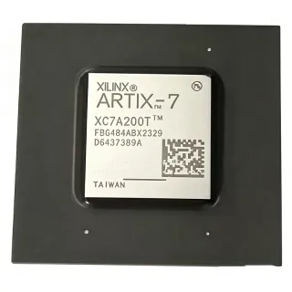
EP3CLS100F484C8 - Cyclone III LS FPGA | Altera / Intel
MPN: EP3CLS100F484C8 ✓ Active| Qty | Unit Price | Extended |
|---|---|---|
| 1 | $218.5 | $218.50 |
| 10 | $196.8 | $1,968.00 |
| 100 | $175.2 | $17,520.00 |
| 500 | $162.3 | $81,150.00 |
| 1,000 | $148.45 | $148,450.00 |
EP3CLS100F484C8 Overview
An FPGA is a semiconductor device whose logic fabric and interconnects are reconfigured by the user after manufacturing. FPGAs occupy the programmable-logic portion of the integrated circuit hierarchy: FPGA -> programmable logic device -> integrated circuit. Unlike ASICs, they can be updated in the field, which makes them useful for prototyping, low-to-medium production, and systems where standards change quickly. The EP3CLS100F484C8 is the 100,000-logic-element-class member of the Cyclone III LS series, designed for applications that need high logic density without the cost or power of an ASIC.
Key features include 100,448 logic elements, 4,451,328 RAM bits, and 278 user I/Os. The device is a commercial-grade part in the Altera/Intel ordering code, where C indicates commercial temperature and 8 indicates speed grade 8. According to distributor and cross-reference data, the FPGA is built on a 65nm process and is rated for 1.2V core operation, with an FPGA performance indicator of 402MHz in the Cyclone III LS family. The 484-ball FBGA package provides enough pins for wide memory buses and many parallel I/O channels.
The Cyclone III LS family is distinguished from the standard Cyclone III family by lower power and the LS security-related features; the exact feature set and I/O standard support are defined in the Cyclone III and Cyclone III LS device handbooks. From a system perspective, the EP3CLS100F484C8 provides a reconfigurable parallel computing fabric that can implement RTL logic, soft processors, DSP datapaths, and state-machine controllers in one device. It requires an external configuration device or JTAG download at power-up because it is SRAM-based.
Typical applications for this FPGA include industrial motor control and factory automation, networking and Ethernet bridging, machine vision and video processing, medical imaging equipment, high-performance test-and-measurement instruments, and compute/network acceleration. The high I/O count and 100K logic capacity allow designers to integrate multiple discretely implemented functions onto one programmable platform, reducing total system component count.
A key design consideration is that the EP3CLS100F484C8 requires a clean 1.2V core supply and correct power-up configuration sequencing. Use a serial configuration device such as the EPCS or EPCQ family, or download the bitstream through JTAG during development. Thermal dissipation from an FPGA this size also requires proper BGA layout, sufficient copper planes, and air flow in the final enclosure.
This page synthesizes distributor pricing, availability, drop-in family alternatives, and practical design guidance not found in a single datasheet chapter, making it a useful engineering research resource before committing to a full Intel/Altera documentation review.
Drop-in alternatives for EP3CLS100F484C8 — same package, pin-to-pin compatible. Different-package parts requiring PCB rework are excluded.
Variants in this series
Same-series models that are drop-in compatible with EP3CLS100F484C8 (same form factor and footprint) — differing in Process Technology, Package, Speed Grade, RoHS Status, PLLs.
Quick Comparison Tool — Select alternative parts for side-by-side comparison:
EP3CLS100F484C7N
✅ Drop-In✓ In Stock
$495.8 / Unit
View Datasheet →EP3CLS100F484C7
✅ Drop-In ⚠️ 参数待验证✓ In Stock
$62.8 / Unit
View Datasheet →EP3CLS100F484I7N
✅ Drop-In ⚠️ 参数待验证✓ In Stock
$67.9 / Unit
View Datasheet →EP3CLS100F484I7
✅ Drop-In ⚠️ 参数待验证✓ In Stock
$113.6 / Unit
View Datasheet →EP3CLS100F484C8N
✅ Drop-In ⚠️ 参数待验证✓ In Stock
$115.4 / Unit
View Datasheet →EP3CLS100F484C8 Maximum Ratings & Electrical Characteristics
| Product Type | FPGA - Field Programmable Gate Array |
| Series | Cyclone III LS |
| Number of Logic Elements | 100448 |
| Total RAM Bits | 4451328 bits |
| Number of User I/O | 278 |
| Core Supply Voltage | 1.2 V |
| Process Technology | 65 nm |
| Maximum Clock Frequency Rating | 402 MHz |
| Package Type | FBGA-484 |
| Number of Pins | 484 |
| Package Shape | Square |
| Terminal Form | Ball |
| Mounting Type | Surface Mount |
| Speed Grade | 8 (from C8 ordering code) |
| Temperature Grade | Commercial (C) |
| RoHS Status | unknown |
EP3CLS100F484C8 square Pin Configuration Guide
Pin configuration for EP3CLS100F484C8 (square package). This digital IC includes GPIO, communication interfaces (UART, SPI, I2C), and power pins. Refer to the manufacturer datasheet for alternate pin functions and configuration options. Essential for embedded system design and PCB layout.

No detailed pinout data available for EP3CLS100F484C8.
Refer to the datasheet for full pin configuration.
Typical Applications
EP3CLS100F484C8 is suitable for 6 applications: Industrial Automation and Machine Control, Wired Networking and Ethernet Bridging, Machine Vision and Video Processing, Medical Imaging and Patient Monitoring, Test and Measurement Instruments, Compute and Network Acceleration.
Industrial Automation and Machine Control
The EP3CLS100F484C8 provides 100,448 logic elements, enough to implement multi-axis motor-control loops, fieldbus interfaces, and safety logic in a single 484-ball FPGA. The 278 user I/Os allow glueless connection to position encoders, gate-driver signals, and HMI bridges. 4,451,328 RAM bits are sufficient for local data logging and small Ethernet packet buffers. When used as a central controller, its 1.2V core supply reduces system power without sacrificing 65nm performance. The C suffix supports 0°C to 85°C, adequate for many indoor industrial applications; for extreme environments consider I-suffix variants. Typical companions include an external EPCS/EPCQ configuration flash and an isolated transceiver for fieldbus communications.
Recommended
Wired Networking and Ethernet Bridging
With 4,451,328 RAM bits and a rated 402MHz FPGA performance indicator, the EP3CLS100F484C8 can implement Ethernet MAC bridging, frame parsing, traffic classification, and queue management logic in one device. The 278 user I/Os provide sufficient pins for GMII/RGMII PHY connections, control-plane interfaces, and sideband management buses. Using the FPGA for packet preprocessing offloads a host CPU and makes the product field-upgradable when protocol definitions change. The 65nm 1.2V core reduces power compared to older 1.5V FPGAs, which is important in compact networking equipment. In this application, place the FPGA close to PHY devices, keep clock routing length-matched, and couple it with an EPCS/EPCQ flash for autonomous boot.
Recommended
Machine Vision and Video Processing
A 100K-logic-element FPGA such as the EP3CLS100F484C8 is suitable for real-time image sensor interface, Bayer demosaic, color-space conversion, and low-latency feature extraction. The device’s 278 user I/Os enable parallel connections to CMOS imagers, DDR memory, and display controllers without requiring an external video bridge. Because the FPGA fabric performs pixel operations in parallel, it can maintain full-frame throughput at high resolutions while leaving a host processor free for higher-level algorithms. Its commercial temperature grade fits indoor machine-vision enclosures and test benches. The 1.2V core helps manage the thermal load in cameras and smart-vision modules. Use an external image sensor with a parallel or LVDS interface and a configuration flash for standalone boot.
Recommended
Medical Imaging and Patient Monitoring
In medical imaging systems such as ultrasound front ends, optical coherence tomography engines, and diagnostic monitoring equipment, the EP3CLS100F484C8 can perform real-time digital filtering, demodulation, and data formatting before sending results to a CPU. The 65nm low-power process keeps heat dissipation low in sealed medical housings, while the 100K logic elements and 278 I/O allow integration of multiple channels. The 4,451,328 RAM bits support line buffers and small scan-conversion tables. For medical bench equipment and hospital devices that do not require extended automotive temperature, the C-suffix variant is acceptable; however, system-level safety certifications and EMC requirements must be validated separately. Design with clean power planes and place bypass capacitors close to the FPGA core balls.
Recommended
Test and Measurement Instruments
The EP3CLS100F484C8 is well suited for oscilloscopes, logic analyzers, spectrum analyzers, and protocol analyzers where high-I/O parallel data acquisition and trigger logic are required. Its 278 user I/Os allow direct connection to multiple ADC/DAC devices, front-panel controls, and high-speed backplanes. The reconfigurable fabric enables custom trigger patterns, decimation filters, and real-time data reduction, which reduces the burden on an embedded processor. 4,451,328 RAM bits are useful for acquisition buffers and FFT frame packaging. In test equipment, use a low-jitter clock source and carefully route high-speed data buses into the FPGA. The commercial temperature grade is sufficient for benchtop instruments operating in a controlled lab environment.
Recommended
Compute and Network Acceleration
In server and edge-computing applications, the EP3CLS100F484C8 can accelerate packet classification, hashing, data deduplication, and message parsing while a host CPU manages higher-level processing. The 1.2V core and 65nm process provide a balance of logic density and power for PCIe or Ethernet-attached accelerator cards. 100,448 logic elements can hold multiple soft pipeline stages, and 278 I/O are enough to interface with memory buffers, PHYs, and host bridge logic. Because FPGAs are reprogrammable, acceleration algorithms can be updated without hardware changes, which is advantageous for evolving protocols. This device is not meant for high-end 100G SmartNIC designs but works well in cost-sensitive 1/10G acceleration paths and embedded compute modules. Use configuration flash and a suitable power converter for the 1.2V core.
Recommended
Recommended Products Summary
Engineering reference data for EP3CLS100F484C8 — comparison, design guidance, and compliance information.
Selection Guide
Comparison with Alternatives
| Parameter | This Product | EP3CLS100F484C7N | EP3CLS100F484C7 | EP3CLS100F484I7N | EP3CLS100F484I7 | EP3CLS100F484C8N |
|---|---|---|---|---|---|---|
| Brand | Altera | Altera | Altera | Altera | Altera | Altera |
| Package | FBGA-484 | FBGA-484 - same | FBGA-484 - same | FBGA-484 - same | FBGA-484 - same | FBGA-484 - same |
| Number of Logic Elements | 100448 | 100448 | 100448 | 100448 | 100448 | 100448 |
| Total RAM Bits | 4451328 | 4451328 | 4451328 | 4451328 | 4451328 | 4451328 |
| Number of User I/O | 278 | 278 | 278 | 278 | 278 | 278 |
| Core Supply Voltage | 1.2V | 1.2V | 1.2V | 1.2V | 1.2V | 1.2V |
| Speed Grade (ordering code) | 8 (C8) | 7 (C7N) | 7 (C7) | 7 (I7N) | 7 (I7) | 8 (C8N) |
| Temperature Grade | C (Commercial) | C (Commercial) | C (Commercial) | I (Industrial) | I (Industrial) | C (Commercial) |
| Pb-free N suffix | No N in MPN | Yes (N suffix) | No | Yes (N suffix) | No | Yes (N suffix) |
Key Differentiators
- Commercial C-suffix part targets indoor, cost-sensitive systems (vs EP3CLS100F484I7N)
- Speed grade 8 is a lower performance but potentially more economical grade (vs EP3CLS100F484C7N)
- Non-N suffix may simplify legacy SnPb soldering process reuse (vs EP3CLS100F484C8N)
Design Notes
The EP3CLS100F484C8 core is a 1.2V SRAM FPGA. Provide a low-impedance 1.2V core rail plus separate VCCO supplies for each I/O bank according to the Cyclone III pin connection guidelines. Place 100nF ceramic capacitors as close as possible to the FPGA power/ground balls and add bulk capacitance on the board. Sizing the power distribution network should be based on the final design toggle rate; do not simply copy a low-density FPGA decoupling layout.
Cyclone III LS devices are SRAM-based and require an external configuration source after power-up. Plan for active serial configuration using an EPCS/EPCQ configuration device, or use JTAG during development. At power-on, drive nCONFIG low until the power supplies have stabilized, then release it to start configuration. Protect the configuration device from accidental writes if in-system update is not used.
The 484-ball FBGA package uses a BGA land pattern with hidden rows. Use the official Intel/Altera footprint and pin files to generate the PCB symbol, and route inner balls using via-in-pad or escape vias under the component when necessary. Provide a continuous ground plane beneath the FPGA and minimize the distance between vias and power balls to reduce inductance.
For high-speed source-synchronous interfaces, keep clock and data trace lengths matched within the values recommended by the interface standard. Add series termination resistors near the FPGA outputs when driving long traces or multiple loads. Unused user I/O pins should be assigned to tri-state in the Quartus assignment editor to prevent bus contention during configuration and after boot.
Compliance Information
No explicit compliance declarations were provided in the verified web data. The absence of an 'N' in the part number may indicate a non-lead-free finish, but this must be confirmed with the manufacturer or an authorized distributor.