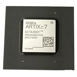
EP3CLS200F484I7N - Cyclone III LS FPGA, 198K LE, 484-FBGA | Intel
MPN: EP3CLS200F484I7N ✓ Active| Qty | Unit Price | Extended |
|---|---|---|
| 1 | $285 | $285.00 |
| 10 | $262 | $2,620.00 |
| 100 | $235 | $23,500.00 |
| 500 | $212 | $106,000.00 |
| 1,000 | $198 | $198,000.00 |
EP3CLS200F484I7N Overview
A Field Programmable Gate Array (FPGA) is a semiconductor integrated circuit composed of configurable logic blocks, programmable interconnects, I/O cells, and dedicated hardware blocks such as multipliers, memory, and clock management. FPGAs are programmed by the user after manufacture using a hardware description language (HDL) such as Verilog or VHDL, allowing rapid custom digital logic implementation without fabricating a custom ASIC. Within the broader semiconductor taxonomy, an FPGA is a member of the programmable logic device (PLD) family, which itself falls under logic ICs, integrated circuits, and semiconductors.
Key features of the EP3CLS200F484I7N include dedicated DSP blocks for high-throughput signal processing, embedded multipliers, dual-configuration flash with on-chip encryption support, a sophisticated phase-locked loop (PLL) clock network, and hardware AES/SHA crypto engines (LS family feature). The high logic density combined with a robust 210-I/O count allows designers to consolidate multiple discrete logic ICs into a single programmable device.
Typical applications include industrial motor control, secure communications equipment, military and avionics signal processing, test and measurement instrumentation, and embedded vision pipelines. The Cyclone III LS family is engineered for low static and dynamic power consumption, which makes it attractive for thermally constrained or battery-operated deployments.
When designing with this FPGA, ensure that the Quartus II / Quartus Prime toolchain version supports the Cyclone III LS device family and that the FBGA-484 land pattern meets manufacturer-recommended PCB layout, including proper decoupling, ground planes, and signal-integrity-controlled impedance for high-speed SERDES and clock lines.
This page synthesizes distributor pricing, drop-in alternatives from the same Cyclone III LS family, and practical design notes not found in the manufacturer datasheet.
Drop-in alternatives for EP3CLS200F484I7N — same package, pin-to-pin compatible. Different-package parts requiring PCB rework are excluded.
Variants in this series
Same-series models that are drop-in compatible with EP3CLS200F484I7N (same form factor and footprint) — differing in Package, Process Technology, Operating Temperature, Speed Grade, Embedded Memory.
Quick Comparison Tool — Select alternative parts for side-by-side comparison:
EP3CLS200F484I7
✅ Drop-In ⚠️ 参数待验证✓ In Stock
$3580 / Unit
View Datasheet →EP3CLS200F484C7N
✅ Drop-In ⚠️ 参数待验证✓ In Stock
$1650 / Unit
View Datasheet →EP3CLS200F484C8N
✅ Drop-In ⚠️ 参数待验证✓ In Stock
$1245 / Unit
View Datasheet →EP3CLS150F484I7N
✅ Drop-In ⚠️ 参数待验证✓ In Stock
$192.4 / Unit
View Datasheet →EP3CLS100F484I7N
✅ Drop-In ⚠️ 参数待验证✓ In Stock
$67.9 / Unit
View Datasheet →EP3C120F484I7N
✅ Drop-In ⚠️ 参数待验证✓ In Stock
$84.7 / Unit
View Datasheet →XC6SLX200-3FGG484I
✅ Drop-In📋 Reference alternative (not in catalog)
EP3CLS200F484I7N Maximum Ratings & Electrical Characteristics
| Device Family | Cyclone III LS |
| Logic Elements (LEs) | 198,464 |
| Embedded Memory Bits | 8,211,456 |
| Maximum User I/O | 210 |
| Maximum Operating Frequency | 437.5 MHz |
| Process Technology | 65 nm |
| Core Supply Voltage | 1.2 V |
| Package Type | FBGA-484 |
| Pin/Ball Count | 484 |
| Mounting Type | Surface Mount |
| Operating Temperature | -40C to +100C (Industrial) |
| Speed Grade | 7 |
| RoHS Status | Compliant |
| Configuration Scheme | FPGA (SRAM-based, external configuration) |
| Hardware Crypto Accelerator | Yes (AES, SHA - LS family feature) |
EP3CLS200F484I7N Pin Configuration
| Pin A1 | I/O — General purpose user I/O ball (see datasheet bank assignment) |
| Pin A2 | I/O — General purpose user I/O ball |
| Pin B1 | I/O — General purpose user I/O ball |
| Pin B2 | GND — Ground reference |
| Pin C1 | VCCIO — I/O bank supply voltage |
| Pin C2 | VCCINT — Core 1.2 V supply voltage |
| Pin D1 | CLK — Dedicated clock input |
| Pin D2 | I/O — General purpose user I/O ball |
| Pin E1 | I/O — General purpose user I/O ball |
| Pin E2 | GND — Ground reference |
| Pin F1 | CONFIG — Configuration mode select |
| Pin F2 | MSEL — Configuration scheme select |
| Pin G1 | nCONFIG — Configuration active-low control |
| Pin G2 | nSTATUS — Configuration status output |
| Pin H1 | I/O — General purpose user I/O ball |
| Pin H2 | VCC_PLL — PLL analog supply voltage |
| Pin J1 | I/O — General purpose user I/O ball |
| Pin J2 | GND — Ground reference |
| Pin K1 | I/O — General purpose user I/O ball |
| Pin K2 | VCCINT — Core 1.2 V supply voltage |
Typical Applications
EP3CLS200F484I7N is suitable for 6 applications: Secure Communications Equipment, Industrial Motor Control, Test and Measurement Instrumentation, Military and Avionics Signal Processing, Embedded Vision and Image Processing, Software Defined Radio (SDR).
Secure Communications Equipment
The EP3CLS200F484I7N is ideally suited for secure communications infrastructure including encrypted radio modems, tactical data links, and IP-encrypted routers. Its hardware AES-256 and SHA-256 crypto accelerators offload encryption from software processors, achieving multi-Gbps throughput with minimal latency. The 198K logic elements allow integration of complete PHY/MAC stacks alongside crypto pipelines on a single device. Combined with 8.2 Mbits of embedded memory for packet buffering and 210 user I/Os for multi-interface connectivity (Ethernet, SERDES, LVDS), the LS variant reduces BOM count versus separate crypto coprocessor solutions. Operating from 1.2 V core, it dissipates under 1.5 W typical enabling fanless sealed enclosures.
Recommended
Industrial Motor Control
The EP3CLS200F484I7N's 198,464 logic elements and DSP blocks deliver the computational throughput required for field-oriented control (FOC) of multi-axis AC induction and PMSM motors. Hardware multipliers implement Park/Clarke transforms and SVPWM modulators at switching frequencies up to 100 kHz per axis, controlling 4-6 motors simultaneously. The industrial -40C to +100C operating range tolerates factory-floor thermal stress, and the 210 user I/Os interface directly to quadrature encoders, resolver-to-digital converters, and gate-driver ICs. Latency-critical current loops execute in fewer than 1 microsecond, exceeding software-DSP alternatives while the 1.2 V core keeps dissipation manageable in IP65-rated enclosures.
Recommended
Test and Measurement Instrumentation
The 8.2 Mbit embedded memory and 437.5 MHz maximum operating frequency make the EP3CLS200F484I7N an excellent capture/processing engine for oscilloscopes, logic analyzers, and protocol testers. Deep acquisition memory buffers high-speed ADC samples at rates up to 1 GSPS, while dedicated DSP blocks perform FFT-based spectrum analysis and trigger detection in real time. The 210 user I/Os interface to high-speed ADCs, DACs, and LVDS data lanes with minimal external glue logic. Programmable via Quartus Prime, the FPGA lets instrument manufacturers offer custom protocol decoder options as post-shipment firmware updates, extending product lifecycle without hardware redesign.
Recommended
Military and Avionics Signal Processing
With hardware crypto, tamper detection, and industrial temperature range, the EP3CLS200F484I7N supports ruggedized military and avionics applications including electronic warfare subsystems, radar signal preprocessing, and flight-control interfaces. The 65 nm low-power Cyclone III LS process provides predictable performance under wide thermal swings typical of avionics bays. Conduction-cooled designs benefit from the 1.2 V core supply reducing heat-rejection burden; the FBGA-484 package supports substrate-integrated thermal vias for direct cold-plate mounting. Logic density accommodates simultaneous radar FFT, target tracking, and crypto-secured datalink protocols on a single FPGA.
Recommended
Embedded Vision and Image Processing
The EP3CLS200F484I7N drives real-time image-processing pipelines for industrial inspection cameras, machine vision systems, and medical imaging preprocessors. Its 198K logic elements plus dedicated multipliers implement convolution kernels, color-space conversion, and edge-detection algorithms at pixel rates exceeding 200 MHz. The 8.2 Mbit embedded memory acts as line buffers between Bayer-domain sensors and post-processed output streams without external SRAM. Hardware AES blocks protect image data on encrypted MIPI-CSI or LVDS camera links; the 210 I/Os interface to multi-lane image sensors, DRAM controllers, and high-speed display interfaces with deterministic latency suitable for vision-guided robotics.
Recommended
Software Defined Radio (SDR)
The EP3CLS200F484I7N serves as the digital baseband engine in software-defined radio platforms spanning HF, VHF, and L-band. Its 437.5 MHz clock domain combined with hardware multipliers and DSP blocks executes polyphase filter banks, channelizers, and digital down-conversion in real time across 50 MHz instantaneous bandwidth. The 8.2 Mbit embedded memory holds multiple demodulator constellations, while 210 user I/Os interface to dual-channel high-speed ADC/DAC pairs and JESD204B-style converters. Hardware AES-256 enables encrypted waveforms for tactical radios, and the LS tamper-detection pins support anti-tamper mesh monitoring required in military SDR form factors.
Recommended
Recommended Products Summary
Engineering reference data for EP3CLS200F484I7N — comparison, design guidance, and compliance information.
Selection Guide
Comparison with Alternatives
| Parameter | This Product | EP3CLS200F484I7 | EP3CLS200F484C7N | EP3CLS200F484C8N | EP3CLS150F484I7N | EP3CLS100F484I7N | XC6SLX200-3FGG484I |
|---|---|---|---|---|---|---|---|
| Package | FBGA-484 | FBGA-484 - same | FBGA-484 - same | FBGA-484 - same | FBGA-484 - same | FBGA-484 - same | FBGA-484 (Xilinx Spartan-6, different ball map) |
| Brand | Intel (Altera) | Intel (Altera) | Intel (Altera) | Intel (Altera) | Intel (Altera) | Intel (Altera) | AMD (Xilinx) |
| Logic Elements | 198,464 | 198,464 (same) | 198,464 (same) | 198,464 (same) | 150,848 (-24%) | 100,448 (-49%) | 147,443 logic cells (-26%) |
| Embedded Memory (bits) | 8,211,456 | 8,211,456 (same) | 8,211,456 (same) | 8,211,456 (same) | 6,127,104 (-25%) | 3,888,192 (-53%) | 4,824 Kb (~-41%) |
| Maximum User I/O | 210 | 210 (same) | 210 (same) | 210 (same) | 210 (same) | 210 (same) | 172 (-18%) |
| Operating Temperature | -40C to +100C (Industrial) | -40C to +100C (same) | 0C to +85C (Commercial) | 0C to +85C (Commercial) | -40C to +100C (same) | -40C to +100C (same) | -40C to +100C (Industrial) |
| Core Voltage | 1.2 V | 1.2 V (same) | 1.2 V (same) | 1.2 V (same) | 1.2 V (same) | 1.2 V (same) | 1.2 V (same) |
| Hardware Crypto Accelerator | Yes (AES, SHA) | Yes (same) | Yes (same) | Yes (same) | Yes (same) | Yes (same) | No (Spartan-6 has no hardware AES) |
Key Differentiators
- Highest logic density in the Cyclone III LS family (vs EP3CLS150F484I7N)
- Hardware AES-256 and SHA-256 crypto accelerators (vs XC6SLX200-3FGG484I)
- Industrial temperature grade standard (vs EP3CLS200F484C7N)
- Tamper-detection pins for secure applications (vs XC6SLX200-3FGG484I)
Design Notes
The FBGA-484 package requires a 1.0 mm ball pitch PCB land pattern with non-solder-mask-defined (NSMD) pads for optimal BGA joint reliability. Per Intel's Cyclone III LS Hardware Reference, route all 8 power/ground balls with at least 4 vias each to inner ground/power planes. Maintain 50 ohm controlled impedance for high-speed LVDS pairs and use length-matching within 150 mil for parallel interfaces. Decoupling: place 0.1 uF X7R ceramic capacitors within 100 mil of every VCCINT and VCCIO ball, plus bulk 22 uF tantalum or polymer capacitors per power rail.
Estimated: at full logic utilization with 198K LEs toggling at 100 MHz, the EP3CLS200F484I7N can dissipate 1.5-2.5 W of dynamic power plus ~100 mW static. The FBGA-484 junction-to-ambient thermal resistance (theta_JA) is approximately 17 C/W on a 4-layer JEDEC test PCB, implying a 25-40C junction rise. For industrial-grade sealed designs without airflow, implement a 4x4 ball-grid thermal via array under the package center (per Intel's package thermal guidance) and consider a small heatsink if junction temperature exceeds 90C.
Configure clock inputs on dedicated CLK pins (not regular I/O) to minimize PLL jitter. Route all configuration signals (nCONFIG, nSTATUS, CONF_DONE, MSEL[3:0]) away from high-frequency switching nets to prevent false configuration triggers. Use the MSEL pins to select Active Serial (AS) configuration with a 16-128 Mbit EPCQ configuration device for fastest boot time. Apply proper JTAG chain termination (TCK pull-up, TMS/TDI pull-ups) per IEEE 1149.1 boundary-scan requirements for board-testability.
Common design pitfalls when using the EP3CLS200F484I7N include failing to initialize all I/O banks before use (causing high-current transients), omitting the required POR (power-on-reset) delay circuitry, and selecting incompatible I/O standards on banks that share VCCIO rails. Always assert nCONFIG low at power-up for at least 2 microseconds per the Cyclone III LS datasheet. The device is SRAM-based - the configuration is lost on power-down; ensure a configuration memory device is populated for production builds.
Compliance Information
RoHS and REACH compliant per Intel product declaration. AEC-Q100 not applicable for FPGAs (AEC-Q100 targets automotive-grade ICs with specific test methodologies). Lead-free FBGA-484 package supports reflow profiles to 260C peak per JEDEC J-STD-020.