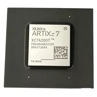
EP2C35F484I8 - 33,216-Cell, 1.2V Cyclone II FPGA | Intel
MPN: EP2C35F484I8 ✗ End of Life| Qty | Unit Price | Extended |
|---|---|---|
| 1 | $163.7027 | $163.70 |
| 10 | $163.7027 | $1,637.03 |
| 100 | $163.7027 | $16,370.27 |
| 500 | $163.7027 | $81,851.35 |
| 1,000 | $163.7027 | $163,702.70 |
EP2C35F484I8 Overview
A field-programmable gate array is a programmable semiconductor containing configurable logic blocks, routing resources, and specialized functional blocks. Unlike a fixed application-specific integrated circuit, an FPGA can implement changing digital logic, interface protocols, control functions, and signal-processing datapaths through a user-generated configuration. Within programmable logic, the hierarchy is FPGA, programmable logic IC, configurable logic device, and integrated circuit. The Cyclone II family combines high logic capacity with embedded memory resources for cost-sensitive digital systems.
The headline capacity of 33,216 logic cells supports substantially larger state machines, parallel datapaths, and multi-interface bridges than smaller programmable devices. Its 483,840 memory bits provide on-chip storage for FIFOs, lookup tables, buffers, and control records. A 322-I/O budget permits connection to numerous external memories, data converters, communications peripherals, and control signals. The 1.2 V core supply and 484-FBGA package are central to power-distribution, signal-integrity, and board-layout decisions.
The EP2C35 device architecture is configured after board assembly through an external configuration process; exact supported configuration modes and pins must be obtained from the complete manufacturer datasheet before schematic release. The supplied datasheet excerpt states that the EP2C35 I/O count includes 16 dedicated clock pins that can also be used as data inputs. Clock planning therefore should distinguish package I/O capacity from general-purpose user-I/O requirements rather than treating all 322 pins as identical.
Typical applications include industrial automation controllers, communications-interface equipment, test and measurement systems, and digital-video or display controllers. These systems benefit from parallel processing, reconfigurable interfaces, and the device's 33,216-cell capacity, 483,840 embedded memory bits, and 322 I/Os. Designers must still validate timing closure, configuration circuitry, termination, decoupling, and signal integrity against the target speed grade and complete Cyclone II datasheet.
The most important procurement concern is that the supplied search identifies this mature Cyclone II device but provides no explicit lifecycle statement. Treat lifecycle status as unknown until confirmed from an official Intel product record. No verified cross-reference result establishes a pin-compatible drop-in replacement, so alternatives are limited rather than padded with functional or cross-package devices.
This data synthesis adds verified purchasing links, package-aware replacement analysis, application guidance, and clearly marked datasheet gaps beyond a typical distributor listing. Prices are quoted as of 2026-09-08 from the only supplied unit-price snippet, while stock and lead time remain source-specific.
Drop-in alternatives for EP2C35F484I8 — same package, pin-to-pin compatible. Different-package parts requiring PCB rework are excluded.
Variants in this series
Same-series models that are drop-in compatible with EP2C35F484I8 (same form factor and footprint) — differing in Operating Temperature, Process Technology, Package, RoHS Status, Logic Elements.
Quick Comparison Tool — Select alternative parts for side-by-side comparison:
EP2C35F484C8N
✅ Drop-In ⚠️ 参数待验证✓ In Stock
$65 / Unit
View Datasheet →EP2C35F484C8
✅ Drop-In ⚠️ 参数待验证✓ In Stock
$28.9 / Unit
View Datasheet →EP2C35F484C7N
✅ Drop-In ⚠️ 参数待验证✓ In Stock
$85.2 / Unit
View Datasheet →EP2C35F484C7
✅ Drop-In ⚠️ 参数待验证✓ In Stock
$54.25 / Unit
View Datasheet →EP2C35F484C6N
✅ Drop-In✓ In Stock
$118.2 / Unit
View Datasheet →EP2C35F484I8 Maximum Ratings & Electrical Characteristics
| Product Type | Field Programmable Gate Array (FPGA) |
| Logic Family | Cyclone II |
| Process Technology | CMOS |
| Logic Cells | 33216 |
| Logic Cells or Logic Blocks per DigiChip Snippet | 2100 |
| Embedded Memory | 483840 bit |
| User I/O Count | 322 |
| Supply Voltage | 1.2 V |
| Maximum Frequency | 402.58 MHz |
| Package Pin Count | 484 |
| Package Type | FBGA-484 |
| Mounting Type | Surface Mount |
| Operating Temperature | 0 °C to 85 °C |
| Ordering Temperature Grade | Industrial grade |
| Packaging Format | Tray |
| RoHS Status | unknown |
| REACH Status | unknown |
| AEC-Q100 Qualification | not_qualified |
EP2C35F484I8 fbga-484 Pin Configuration Guide
Pin configuration for EP2C35F484I8 (fbga-484 package). This digital IC includes GPIO, communication interfaces (UART, SPI, I2C), and power pins. Refer to the manufacturer datasheet for alternate pin functions and configuration options. Essential for embedded system design and PCB layout.

No detailed pinout data available for EP2C35F484I8.
Refer to the datasheet for full pin configuration.
Typical Applications
EP2C35F484I8 is suitable for 6 applications: Industrial Automation Controllers, Communications Interface Equipment, Test and Measurement Systems, Digital Video and Display Controllers, Reconfigurable Control and Interface Platform, Embedded Data-Acquisition Hub.
Industrial Automation Controllers
EP2C35F484I8 fits industrial automation controllers that require parallel deterministic logic and many external connections. Its 33,216 logic cells can implement motion sequencing, I/O handling, communications bridges, and supervisory control in one programmable device, while 483,840 embedded memory bits support FIFOs, protocol buffers, and timing tables. The 322-I/O interface can connect field buses, sensors, motor-control peripherals, and service interfaces without duplicating all functions in discrete logic. Its verified 1.2 V supply and 0 °C to 85 °C operating range make it plausible for controlled industrial enclosures, but timing closure, supported I/O standards, and configuration details must be confirmed. The 484-FBGA package also requires controlled impedance, BGA escape routing, robust decoupling, and a stable configuration circuit; an industrial design should not treat same-package Cyclone II variants as drop-in substitutes without checking every ball and speed-grade condition.
Recommended
Communications Interface Equipment
EP2C35F484I8 is appropriate for communications equipment that combines packet handling, interface adaptation, and timing control. The FPGA's 33,216 logic cells can process parallel datapaths, custom link layers, statistics, and control states, while 483,840 embedded memory bits can hold FIFOs, lookup tables, and transient packet data. Its 322 I/Os provide enough package-level connectivity for multiple low- or high-speed peripheral groups, although 16 clock-capable pins are included in the EP2C35 I/O count according to the supplied datasheet excerpt. Designers should budget pins for clocks, configuration, power-associated signals, and differential interfaces before assuming 322 general-purpose connections. A 1.2 V supply simplifies low-voltage core design, but the complete power sequence, allowed I/O voltages, and supported I/O standards are not present in the verified data. Validate line rates, signal integrity, timing, and configuration reliability from official Cyclone II documentation before release.
Recommended
Test and Measurement Systems
EP2C35F484I8 can support test and measurement platforms that require coordinated acquisition, sequencing, analysis, and instrument control. Its 33,216 logic cells provide capacity for custom trigger engines, timing generators, statistical processing, and interface protocols. The 483,840 embedded memory bits are useful for sample buffering, pattern storage, histograms, and capture windows, while 322 I/Os permit connection to converters, clocks, displays, and communications ports. Arrow lists a 402.58 MHz frequency, but that value should not be treated as a design-specific operating frequency without the associated conditions and timing model. The verified 0 °C to 85 °C range supports typical instrument environments, while the 484-FBGA construction demands careful power integrity, clock distribution, controlled impedance, and thermal analysis. Confirm differential I/O support, bank voltages, configuration circuitry, and device power limits from the complete datasheet before selecting this mature FPGA for new production test equipment.
Recommended
Digital Video and Display Controllers
EP2C35F484I8 is suitable for digital video and display controllers that need parallel pixel processing, timing generation, frame buffering, and format conversion. The 33,216 logic cells can implement color-space conversion, overlays, scaling control, synchronization, and display timing, while the 483,840 embedded-memory capacity supports line buffers, lookup tables, and limited frame data. Its 322 I/Os can serve video ports, memories, control signals, and host interfaces, but the supplied data does not identify supported I/O standards or the number of I/O banks. The 1.2 V core supply must be paired with correctly planned I/O-bank voltages and power sequencing. Because the exact configuration pins, memory interfaces, PLL resources, and speed-grade limits are absent from the excerpts, they require [DATA_NEEDED] verification before schematic release. Use the 484-FBGA package with impedance-controlled escape, length-matched high-speed nets, local decoupling, and clock analysis appropriate to the selected display interface.
Recommended
Reconfigurable Control and Interface Platform
EP2C35F484I8 works well as a reconfigurable platform for products whose interfaces or control algorithms may evolve after deployment. Its 33,216 logic cells accommodate substantial custom control logic, and 483,840 embedded memory bits permit FIFOs, state records, and configurable tables. The 322-I/O resource allows a platform architecture with multiple external interfaces, but dedicated clock and configuration functions must be reserved early. The device's 1.2 V supply and 0 °C to 85 °C operating range support conventional embedded equipment when current and thermal design rules are met. Configuration storage, supported modes, and pin assignments are not present in the verified excerpts, so [DATA_NEEDED] remains for production configuration design. Unlike package sharing, FPGA logic compatibility does not prove electrical or configuration compatibility across orderable suffixes. Evaluate the exact I8 code, complete ball map, firmware tool support, configuration PROM, in-system update strategy, and lifecycle availability before committing the platform to a long production run.
Recommended
Embedded Data-Acquisition Hub
EP2C35F484I8 can serve as the coordination hub in an embedded data-acquisition system, combining multiple converter interfaces, local buffering, timestamping, and host communications. The 33,216 logic cells are enough for parallel control, protocol formatting, filtering, and real-time sequencing, while 483,840 embedded memory bits can hold acquisition windows, calibration tables, and FIFOs. Its 322 I/Os are valuable for connecting several data sources, clocks, controls, and storage devices. However, 16 dedicated clock pins are included in the EP2C35 I/O count, and supported I/O standards, bank limits, and PLL resources are not stated in the supplied data. Design engineers must therefore verify pin compatibility and electrical constraints rather than assume 322 identical general-purpose channels. The 1.2 V supply requires a low-noise power network, and the 484-FBGA package benefits from short decoupling paths and continuous reference planes. Validate converter timing, clock jitter, configuration integrity, and thermal behavior under worst-case acquisition load.
Recommended
Recommended Products Summary
Engineering reference data for EP2C35F484I8 — comparison, design guidance, and compliance information.
Selection Guide
Comparison with Alternatives
| Parameter | This Product | EP2C35F484C8N | EP2C35F484C8 | EP2C35F484C7N | EP2C35F484C7 | EP2C35F484C6N |
|---|---|---|---|---|---|---|
| Brand | Intel / Altera | Intel / Altera | Intel / Altera | Intel / Altera | Intel / Altera | Intel / Altera |
| Package | FBGA-484 | FBGA-484 | FBGA-484 | FBGA-484 | FBGA-484 | FBGA-484 |
| Logic Cells | 33216 | 33216 | 33216 | 33216 | 33216 | 33216 |
| I/O Count | 322 | 322 | 322 | 322 | 322 | 322 |
| Supply Voltage | 1.2 V | 1.2 V | 1.2 V | 1.2 V | 1.2 V | 1.2 V |
| Operating Temperature | 0 °C to 85 °C | Commercial temperature grade | Commercial temperature grade | Commercial temperature grade | Commercial temperature grade | Commercial temperature grade |
| Orderable-Code Relationship | I8 industrial ordering code | C8N ordering code | C8 ordering code | C7N ordering code | C7 ordering code | C6N ordering code |
Key Differentiators
- High logic capacity within the verified Cyclone II family listing (vs EP2C20F484I8N)
- Large embedded-memory resource (vs EP2C20F484I8N)
- Higher package-level I/O capacity (vs EP2C20F484I8N)
- Industrial operating-temperature ordering code (vs EP2C35F484C6N)
Design Notes
Design the 1.2 V rail from the complete manufacturer power specification rather than deriving stability from the nominal value alone. The verified data confirms only a 1.2 V supply; regulator accuracy, current demand, tolerance, sequencing, and auxiliary-rail requirements are [DATA_NEEDED]. Place bulk and local ceramic decoupling close to the FBGA power balls, use a continuous reference plane, and isolate noisy I/O supplies where required. Check regulator response against simultaneous I/O switching, because peak transient demand can exceed average current. Review the latest Cyclone II datasheet and reference-design power tree before schematic release.
Treat the 484-FBGA land pattern and escape routing as release-critical. The supplied excerpts confirm 484 pins but do not provide package dimensions, ball pitch, ball matrix, or recommended via geometry, all of which are [DATA_NEEDED]. Use the exact orderable-package drawing and verified pin assignment; do not reuse a BGA footprint solely because another EP2C35 suffix also has 484 balls. Fan out inner balls through a plane layer, maintain short return paths, use controlled impedance for high-speed routes, and perform assembly-level via, solder-mask, and pad-stack review before fabrication.
Plan clocks, configuration signals, and high-speed interfaces before logic placement. The supplied datasheet excerpt states that the 322 EP2C35 I/O count includes 16 dedicated clock pins that can be used as data inputs, so those balls must not be consumed as if they were 16 unrestricted general-purpose connections. Assign the configuration interface and power-related pins from the exact datasheet, reserve clock inputs early, and length-match routed differential or source-synchronous interfaces according to their chosen I/O standards. The 402.58 MHz value is only a listed device frequency and does not remove the need for a project-specific timing analysis.
Avoid assuming that a 484-ball package or shared Cyclone II family name guarantees a drop-in alternative. Ordering suffixes can represent commercial versus industrial temperature grades, speed grades, lead-free status, or packaging options, and the supplied excerpts do not provide all conditions for every variant. Before authorizing a replacement, compare the complete ball map, I/O-bank assignments, supported standards, power rails, configuration interface, timing model, package drawing, and lifecycle status. No verified cross-brand drop-in equivalent was found; any competitor solution should be treated as a PCB or firmware redesign rather than a field replacement.
Compliance Information
The supplied excerpts do not explicitly state RoHS, REACH, lead-free, halogen-free, or conflict-minerals compliance. The part is not identified as AEC-Q100 qualified and should not be treated as automotive-qualified from the provided data.