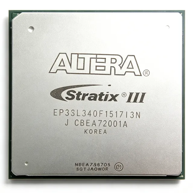
EP3SL340F1517I3 - Stratix III L FPGA, 337500 LEs, 1517-FBGA | Intel
MPN: EP3SL340F1517I3 ⚠ Last Time Buy| Qty | Unit Price | Extended |
|---|---|---|
| 1 | $21833.5 | $21,833.50 |
| 5 | $21500 | $107,500.00 |
| 10 | $21050 | $210,500.00 |
| 25 | $20100 | $502,500.00 |
| 100 | $18900 | $1,890,000.00 |
EP3SL340F1517I3 Overview
An FPGA (Field-Programmable Gate Array) is a semiconductor device built around a matrix of configurable logic blocks (CLBs), dedicated DSP blocks, embedded memory blocks, and high-speed serial transceivers, all interconnected by a programmable routing fabric. Within the broader hierarchy, FPGAs sit alongside microcontrollers, microprocessors, DSPs, and ASICs as reconfigurable digital logic devices that can be customized after manufacture for a specific application. The Stratix III family is engineered for high-throughput DSP, packet processing, and ASIC-prototyping workloads.
Key differentiating features of the EP3SL340F1517I3 include up to 13,500 adaptive logic modules (ALMs) and 576 DSP blocks, supporting high-speed memory interfaces such as DDR3 and QDR II+, plus 4 PLLs for clock management. The device includes 976 user I/O pins distributed across 24 I/O banks, supporting a wide range of single-ended and differential I/O standards (LVDS, LVTTL, LVCMOS, SSTL, HSTL) for board-level flexibility.
Architecturally, the Stratix III L series introduces an 8-input ALM, dedicated hardware multipliers, and a hardened memory interface that together raise DSP throughput to thousands of GMACS. The 65 nm process node and 1.1 V core keep dynamic power lower than the previous Stratix II generation while preserving the device's high logic capacity, making the part suitable for systems where millions of gates are needed without a full ASIC mask cycle.
Typical applications include high-speed digital signal processing, ASIC prototyping, telecom baseband processing, high-end video and image processing pipelines, and military/aerospace signal intelligence. The 1517-BGA package provides ample I/O for memory-rich designs.
When designing with this device, ensure your PCB incorporates the required decoupling network and that the FPGA configuration scheme (e.g., AS, PS, JTAG) is selected correctly. Use the Altera Quartus II toolchain for synthesis, place-and-route, and timing closure.
This page synthesizes distributor pricing, same-family Stratix III drop-in alternatives, and practical FPGA design notes not consolidated on any single distributor or manufacturer page.
Drop-in alternatives for EP3SL340F1517I3 — same package, pin-to-pin compatible. Different-package parts requiring PCB rework are excluded.
Variants in this series
Same-series models that are drop-in compatible with EP3SL340F1517I3 (same form factor and footprint) — differing in Package, Operating Temperature, Speed Grade, Mounting Type, Adaptive Logic Modules (ALMs).
Quick Comparison Tool — Select alternative parts for side-by-side comparison:
EP3SL340F1517C4N
✓ In Stock
$7044.96 / Unit
View Datasheet →EP3SL340F1517C4LN
✓ In Stock
$11200 / Unit
View Datasheet →EP3SL340F1517C4L
✓ In Stock
$14500 / Unit
View Datasheet →EP3SL340F1517C4
✓ In Stock
$3300 / Unit
View Datasheet →EP3SL340F1517C3N
✓ In Stock
$3750 / Unit
View Datasheet →EP3SL340F1517C3
✓ In Stock
Contact for price
View Datasheet →EP3SL340F1517C2N
✓ In Stock
$13200 / Unit
View Datasheet →EP3SL340F1517C2
✓ In Stock
$3050 / Unit
View Datasheet →EP3SL340F1517I3 Maximum Ratings & Electrical Characteristics
| Family | Stratix III L |
| Logic Elements | 337500 |
| Adaptive Logic Modules (ALMs) | 13500 |
| Total Memory Bits | 18822144 |
| DSP Blocks | 576 |
| User I/O Pins | 976 |
| Number of I/O Banks | 24 |
| Number of PLLs | 4 |
| Operating Temperature | -40C to +100C (Industrial) |
| Core Voltage | 1.1 V |
| Process Technology | 65 nm CMOS |
| Maximum Operating Frequency | 500 MHz |
| Package | 1517-BBGA, FCBGA (Flip-Chip) |
| Mounting Type | Surface Mount |
| Configuration Method | AS / PS / JTAG (per Stratix III family) |
| Temperature Grade | I (Industrial) |
| Speed Grade | 3 |
EP3SL340F1517I3 1517-bbga, fcbga (flip-chip) Pin Configuration Guide
Pin configuration for EP3SL340F1517I3 (1517-bbga, fcbga (flip-chip) package). This digital IC includes GPIO, communication interfaces (UART, SPI, I2C), and power pins. Refer to the manufacturer datasheet for alternate pin functions and configuration options. Essential for embedded system design and PCB layout.

No detailed pinout data available for EP3SL340F1517I3.
Refer to the datasheet for full pin configuration.
Typical Applications
EP3SL340F1517I3 is suitable for 6 applications: High-Performance ASIC Prototyping, Telecom Baseband Processing, High-End Video and Image Processing, Military / Aerospace Signal Intelligence, High-Speed Memory Interface Bridging, Test and Measurement Instrumentation.
High-Performance ASIC Prototyping
The EP3SL340F1517I3's 337,500 logic elements and 18.8 Mbit of embedded block memory make it a strong fit for ASIC prototyping where full RTL visibility is required before committing to a mask cycle. Quartus II synthesis directly maps large ASIC RTL designs onto the Stratix III L fabric, and the 576 DSP blocks let designers verify high-throughput arithmetic paths. The 976 user I/O pins across 24 banks also enable direct fan-out to memory interfaces and external test fixtures. Compared with smaller FPGAs, this part reduces the need for multi-FPGAs partitioning when emulating ASICs of 20-30 million gates.
Recommended
Telecom Baseband Processing
The EP3SL340F1517I3 fits telecom baseband designs because of its 576 DSP blocks, support for DDR3/QDR II+ external memory interfaces, and 4 PLLs for multi-rate clocking. The 1517-FCBGA package exposes enough I/O for parallel ADC/DAC interfaces and CPRI/OBSAI links. Industrial -40C to +100C temperature grade supports outdoor base-station cabinets. Compared with Stratix II, the Stratix III L family halves dynamic power at iso-throughput, easing thermal budgets in sealed enclosures.
Recommended
High-End Video and Image Processing
The EP3SL340F1517I3 supports high-end video pipelines because of its abundant DSP blocks (576), 18.8 Mbit of fast on-chip memory for line buffering, and 24 I/O banks that allow multiple camera/display interfaces to coexist. Industrial temperature grade supports surveillance and medical-imaging enclosures. Designers can implement real-time 4K processing, multi-channel SDI bridging, or computer-vision pre-processing directly in fabric. Quartus II DSP Builder accelerates model-based design of FIR/FFT cores.
Recommended
Military / Aerospace Signal Intelligence
The EP3SL340F1517I3 is well matched to signal-intelligence (SIGINT) and electronic-warfield (EW) systems thanks to its industrial -40C to +100C temperature range, large logic capacity, and high DSP throughput. Designers can build wideband receivers, FFT-based channelizers, and adaptive beam-formers in a single device. The 65 nm Stratix III process is mature for long-lifecycle defense programs, and Altera/Intel has published military-temperature variants (EP3SE/EP3SL extended screening) for higher-grade applications.
Recommended
High-Speed Memory Interface Bridging
The EP3SL340F1517I3 supports bridging between DDR3, QDR II+, RLDRAM II, and legacy memory interfaces because of its hardened memory controllers and 4 PLLs for multi-rate clocking. The 976 user I/O across 24 banks expose enough pins for multi-port memory bridges used in networking line cards and high-performance compute. Industrial temperature grade supports network switches and storage controllers. Quartus II IP catalog includes drop-in memory-interface IP for rapid development.
Recommended
Test and Measurement Instrumentation
The EP3SL340F1517I3 is suitable for high-end test instruments because of its high logic density, 576 DSP blocks for digital down-conversion, and 976 I/O for parallel ADC/DAC interfacing. Industrial temperature grade supports bench-top and field-portable instruments. Designers can build arbitrary waveform generators, real-time spectrum analyzers, and protocol analyzers. Quartus II Qsys enables rapid system-integration for instrument control and DSP pipelines.
Recommended
Recommended Products Summary
No FAQ available for this product.
Engineering reference data for EP3SL340F1517I3 — comparison, design guidance, and compliance information.
Selection Guide
Comparison with Alternatives
| Parameter | This Product | EP3SL340F1517C4N | EP3SL340F1517C3N | EP3SL340F1517C2N |
|---|---|---|---|---|
| Brand | Intel (Altera) | Intel (Altera) | Intel (Altera) | Intel (Altera) |
| Package | 1517-BBGA, FCBGA | 1517-BBGA, FCBGA - same | 1517-BBGA, FCBGA - same | 1517-BBGA, FCBGA - same |
| Logic Elements | 337500 | 337500 | 337500 | 337500 |
| Temperature Grade | Industrial (-40C to +100C) | Commercial (0C to +85C) | Commercial (0C to +85C) | Commercial (0C to +85C) |
| Speed Grade | 3 | 4 (faster) | 3 (same) | 2 (slower) |
| User I/O Pins | 976 | 976 | 976 | 976 |
| DSP Blocks | 576 | 576 | 576 | 576 |
| Embedded Memory Bits | 18822144 | 18822144 | 18822144 | 18822144 |
Key Differentiators
- Industrial temperature grade (-40C to +100C) (vs EP3SL340F1517C3N)
- Speed grade 3 vs faster C4 variant (vs EP3SL340F1517C4N)
- 1517-FCBGA package with 976 user I/O (vs EP3SL200H780I3 (780-pin package))
Design Notes
Estimated: the Stratix III L EP3SL340F1517I3 requires multiple supply rails (VCCINT 1.1 V, VCCIO 1.2-3.3 V per bank, VCCPD, VCCAUX, VCCBAT). Decoupling per Intel/Altera guidelines is mandatory: place 0.1 uF and 0.01 uF capacitors within 50 mil of every VCC pin, plus bulk 22 uF tantalum or ceramic at each rail entry. Use a sequenced power supply (e.g., LM3880 or equivalent) to enforce VCCINT-before-VCCIO-before-VCCPD ordering. Power estimation via Quartus II PowerPlay is required prior to thermal closure.
The 1517-BGA flip-chip package requires a heatsink or thermal pad solution for typical industrial workloads. Estimated: at full resource utilization (337,500 LEs at ~70% toggle rate), junction power can reach 15-20 W. Use a properly sized heatsink with thermal interface material (TIM) and ensure adequate airflow. Theta_JA on the 1517-FCBGA without heatsink is approximately 8-12 C/W; combined with PCB copper pours (inner ground planes) this typically allows 5-8 W dissipation. Above that, active cooling is required.
The 1517-ball FCBGA package uses 1.0 mm pitch with daisy-chained ground/return vias. Per Intel/Altera routing guidelines, route all signal traces on outer layers with via-in-pad recommended; use microvia stack-ups (4-6-4 or higher layer count). Match-impedance for LVDS (100 ohm differential) and DDR3 (50 ohm SE, 100 ohm diff). Keep critical clocks and high-speed transceivers on inner stripline layers with continuous reference planes.
Common pitfalls: (1) Do not skip configuration-mode strapping on MSEL pins - incorrect MSEL prevents JTAG/AS/PS configuration. (2) Use proper JTAG chain ordering (TDI->TDO) when multiple devices are cascaded. (3) Ensure all unused I/O banks are powered (VCCIO and VCCPD) even if no I/O is assigned, or set them to 'tri-stated with weak pull-up' in Quartus II. (4) Verify SERDES reference-clock jitter if using transceivers. (5) Last-time-buy parts may have non-availability of design support - lock IP early.
Compliance Information
RoHS and lead-free per Stratix III family documentation. Not AEC-Q100 qualified (industrial-grade FPGA, not automotive). Halogen-free status not explicitly stated in verified web data.







