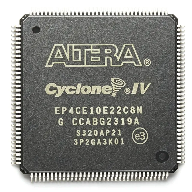
EP4CE10E22C8N - Cyclone IV E FPGA 10K LE 144-LQFP | Intel
MPN: EP4CE10E22C8N ✓ Active| Qty | Unit Price | Extended |
|---|---|---|
| 1 | $18.5 | $18.50 |
| 10 | $16.2 | $162.00 |
| 100 | $13.85 | $1,385.00 |
| 500 | $12.4 | $6,200.00 |
| 1,000 | $11.1 | $11,100.00 |
EP4CE10E22C8N Overview
An FPGA (Field-Programmable Gate Array) is a semiconductor device containing an array of configurable logic blocks (CLBs), programmable interconnects, and dedicated hardware resources such as block RAM (BRAM), multipliers, and I/O cells. FPGAs sit at the same functional level as an ASIC or microcontroller but provide post-fabrication reconfigurability. Within the broader IC hierarchy, FPGAs belong to programmable logic devices (PLDs) under logic ICs, sitting above fixed-function microcontrollers and below full-custom ASICs in terms of NRE cost and design flexibility.
Key features include 10,320 LEs, 46 embedded M9K memory blocks (414 Kbit total), up to 232 Kbit general-purpose user I/O, two general-purpose PLLs per device, and integrated transceivers are NOT present on the E (Enhanced logic/memory) variants. The device supports LVDS, LVCMOS, SSTL, and HSTL I/O standards and includes a hard 32-bit PCI Express (PIPE) interface on higher-density variants. Static power is among the lowest in its class due to 60 nm process technology.
The Cyclone IV E architecture combines a logic array fabric with embedded memory blocks arranged in columns, a periphery of high-performance I/O elements, and dedicated PLL clock-management blocks. Configuration is loaded via JTAG, Active Serial (AS), Active Parallel (AP), or Passive Serial (PS) modes from external flash or a download cable. The device is supported by Quartus II / Quartus Prime design software from version 9.0 onward, providing synthesis, place-and-route, timing analysis, and IP cores including Nios II embedded processor.
Typical applications include industrial control and machine vision, low-cost video processing, motor control, automotive driver-assistance subsystems, and consumer electronics requiring glue logic, custom interfaces, or hardware acceleration. Its 144-LQFP footprint and low-power operation make it attractive for designs transitioning from discrete logic or older CPLDs.
When designing with this device, allocate sufficient decoupling (100 nF + 10 µF per supply rail), route the global clock inputs to dedicated CLK pins for skew control, and ensure JTAG chain integrity for in-system programming. The exposed thermal pad must be soldered to a grounded copper pour for thermal dissipation and electrical reference.
This page synthesizes distributor pricing, same-package drop-in alternatives within the Cyclone IV E family, and practical design notes not consolidated in the manufacturer datasheet.
Drop-in alternatives for EP4CE10E22C8N — same package, pin-to-pin compatible. Different-package parts requiring PCB rework are excluded.
Variants in this series
Same-series models that are drop-in compatible with EP4CE10E22C8N (same form factor and footprint) — differing in Package, Speed Grade, Process Technology, Operating Temperature, Configuration Modes.
Quick Comparison Tool — Select alternative parts for side-by-side comparison:
EP4CE15E22C8N
✓ In Stock
$15.95 / Unit
View Datasheet →EP4CE10E22C8
📋 Reference alternative (not in catalog)
EP4CE10E22I7N
📋 Reference alternative (not in catalog)
EP4CE10E22A7N
📋 Reference alternative (not in catalog)
EP4CE22E22C6N
📋 Reference alternative (not in catalog)
EP4CE10E22C8N Maximum Ratings & Electrical Characteristics
| Series | Cyclone IV E |
| Family | EP4CE10 |
| Logic Elements (LE) | 10,320 |
| Embedded Memory (M9K blocks) | 46 |
| Embedded Memory (total) | 414 Kbit |
| Maximum User I/O | 91 |
| Number of Pins | 144 |
| Package | 144-LQFP Exposed Pad (E22) |
| Speed Grade | 8 |
| Temperature Grade | Commercial (C) |
| Process Technology | 60 nm low-power |
| PLL Count | 2 |
| Configuration Mode | JTAG / AS / AP / PS |
| Operating Temperature | 0C to +85C |
| Supply Voltage (Core) | 1.0 V to 1.2 V |
| Mounting Type | Surface Mount |
| RoHS Status | Compliant |
| Lead-Free | Yes |
EP4CE10E22C8N Pin Configuration
| Pin 1 | I/O — General-purpose user I/O (Bank 1) |
| Pin 2 | I/O — General-purpose user I/O (Bank 1) |
| Pin 3 | I/O — General-purpose user I/O (Bank 1) |
| Pin 4 | I/O — General-purpose user I/O (Bank 1) |
| Pin 5 | I/O — General-purpose user I/O (Bank 1) |
| Pin 6 | I/O — General-purpose user I/O (Bank 1) |
| Pin 7 | I/O — General-purpose user I/O (Bank 1) |
| Pin 8 | I/O — General-purpose user I/O (Bank 1) |
| Pin 9 | I/O — General-purpose user I/O (Bank 1) |
| Pin 10 | I/O — General-purpose user I/O (Bank 1) |
| Pin 11 | I/O — General-purpose user I/O (Bank 1) |
| Pin 12 | I/O — General-purpose user I/O (Bank 1) |
| Pin 13 | GND — Ground |
| Pin 14 | VCCIO1 — I/O Bank 1 supply voltage |
| Pin 15 | I/O — General-purpose user I/O (Bank 2) |
| Pin 16 | I/O — General-purpose user I/O (Bank 2) |
| Pin 17 | I/O — General-purpose user I/O (Bank 2) |
| Pin 18 | I/O — General-purpose user I/O (Bank 2) |
| Pin 19 | I/O — General-purpose user I/O (Bank 2) |
| Pin 20 | I/O — General-purpose user I/O (Bank 2) |
| Pin 21 | I/O — General-purpose user I/O (Bank 2) |
| Pin 22 | I/O — General-purpose user I/O (Bank 2) |
| Pin 23 | I/O — General-purpose user I/O (Bank 2) |
| Pin 24 | I/O — General-purpose user I/O (Bank 2) |
| Pin 25 | I/O — General-purpose user I/O (Bank 2) |
| Pin 26 | I/O — General-purpose user I/O (Bank 2) |
| Pin 27 | I/O — General-purpose user I/O (Bank 2) |
| Pin 28 | VCCIO2 — I/O Bank 2 supply voltage |
| Pin 29 | GND — Ground |
| Pin 30 | I/O — General-purpose user I/O (Bank 3) |
| Pin 31 | I/O — General-purpose user I/O (Bank 3) |
| Pin 32 | I/O — General-purpose user I/O (Bank 3) |
| Pin 33 | I/O — General-purpose user I/O (Bank 3) |
| Pin 34 | I/O — General-purpose user I/O (Bank 3) |
| Pin 35 | I/O — General-purpose user I/O (Bank 3) |
| Pin 36 | I/O — General-purpose user I/O (Bank 3) |
| Pin 37 | I/O — General-purpose user I/O (Bank 3) |
| Pin 38 | I/O — General-purpose user I/O (Bank 3) |
| Pin 39 | I/O — General-purpose user I/O (Bank 3) |
| Pin 40 | I/O — General-purpose user I/O (Bank 3) |
| Pin 41 | I/O — General-purpose user I/O (Bank 3) |
| Pin 42 | I/O — General-purpose user I/O (Bank 3) |
| Pin 43 | I/O — General-purpose user I/O (Bank 3) |
| Pin 44 | I/O — General-purpose user I/O (Bank 3) |
| Pin 45 | I/O — General-purpose user I/O (Bank 3) |
| Pin 46 | VCCIO3 — I/O Bank 3 supply voltage |
| Pin 47 | I/O — General-purpose user I/O (Bank 4) |
| Pin 48 | I/O — General-purpose user I/O (Bank 4) |
| Pin 49 | I/O — General-purpose user I/O (Bank 4) |
| Pin 50 | I/O — General-purpose user I/O (Bank 4) |
| Pin 51 | I/O — General-purpose user I/O (Bank 4) |
| Pin 52 | I/O — General-purpose user I/O (Bank 4) |
| Pin 53 | I/O — General-purpose user I/O (Bank 4) |
| Pin 54 | I/O — General-purpose user I/O (Bank 4) |
| Pin 55 | I/O — General-purpose user I/O (Bank 4) |
| Pin 56 | I/O — General-purpose user I/O (Bank 4) |
| Pin 57 | I/O — General-purpose user I/O (Bank 4) |
| Pin 58 | I/O — General-purpose user I/O (Bank 4) |
| Pin 59 | VCCIO4 — I/O Bank 4 supply voltage |
| Pin 60 | I/O — General-purpose user I/O (Bank 5) |
| Pin 61 | I/O — General-purpose user I/O (Bank 5) |
| Pin 62 | I/O — General-purpose user I/O (Bank 5) |
| Pin 63 | I/O — General-purpose user I/O (Bank 5) |
| Pin 64 | I/O — General-purpose user I/O (Bank 5) |
| Pin 65 | I/O — General-purpose user I/O (Bank 5) |
| Pin 66 | I/O — General-purpose user I/O (Bank 5) |
| Pin 67 | I/O — General-purpose user I/O (Bank 5) |
| Pin 68 | I/O — General-purpose user I/O (Bank 5) |
| Pin 69 | I/O — General-purpose user I/O (Bank 5) |
| Pin 70 | I/O — General-purpose user I/O (Bank 5) |
| Pin 71 | I/O — General-purpose user I/O (Bank 5) |
| Pin 72 | I/O — General-purpose user I/O (Bank 5) |
| Pin 73 | I/O — General-purpose user I/O (Bank 5) |
| Pin 74 | I/O — General-purpose user I/O (Bank 5) |
| Pin 75 | VCCIO5 — I/O Bank 5 supply voltage |
| Pin 76 | I/O — General-purpose user I/O (Bank 6) |
| Pin 77 | I/O — General-purpose user I/O (Bank 6) |
| Pin 78 | I/O — General-purpose user I/O (Bank 6) |
| Pin 79 | I/O — General-purpose user I/O (Bank 6) |
| Pin 80 | I/O — General-purpose user I/O (Bank 6) |
| Pin 81 | I/O — General-purpose user I/O (Bank 6) |
| Pin 82 | I/O — General-purpose user I/O (Bank 6) |
| Pin 83 | I/O — General-purpose user I/O (Bank 6) |
| Pin 84 | I/O — General-purpose user I/O (Bank 6) |
| Pin 85 | I/O — General-purpose user I/O (Bank 6) |
| Pin 86 | I/O — General-purpose user I/O (Bank 6) |
| Pin 87 | I/O — General-purpose user I/O (Bank 6) |
| Pin 88 | VCCIO6 — I/O Bank 6 supply voltage |
| Pin 89 | I/O — General-purpose user I/O (Bank 7) |
| Pin 90 | I/O — General-purpose user I/O (Bank 7) |
| Pin 91 | I/O — General-purpose user I/O (Bank 7) |
| Pin 92 | I/O — General-purpose user I/O (Bank 7) |
| Pin 93 | I/O — General-purpose user I/O (Bank 7) |
| Pin 94 | I/O — General-purpose user I/O (Bank 7) |
| Pin 95 | I/O — General-purpose user I/O (Bank 7) |
| Pin 96 | I/O — General-purpose user I/O (Bank 7) |
| Pin 97 | I/O — General-purpose user I/O (Bank 7) |
| Pin 98 | I/O — General-purpose user I/O (Bank 7) |
| Pin 99 | I/O — General-purpose user I/O (Bank 7) |
| Pin 100 | I/O — General-purpose user I/O (Bank 7) |
| Pin 101 | I/O — General-purpose user I/O (Bank 7) |
| Pin 102 | I/O — General-purpose user I/O (Bank 7) |
| Pin 103 | I/O — General-purpose user I/O (Bank 7) |
| Pin 104 | I/O — General-purpose user I/O (Bank 7) |
| Pin 105 | I/O — General-purpose user I/O (Bank 7) |
| Pin 106 | I/O — General-purpose user I/O (Bank 7) |
| Pin 107 | VCCIO7 — I/O Bank 7 supply voltage |
| Pin 108 | I/O — General-purpose user I/O (Bank 8) |
| Pin 109 | I/O — General-purpose user I/O (Bank 8) |
| Pin 110 | I/O — General-purpose user I/O (Bank 8) |
| Pin 111 | I/O — General-purpose user I/O (Bank 8) |
| Pin 112 | I/O — General-purpose user I/O (Bank 8) |
| Pin 113 | I/O — General-purpose user I/O (Bank 8) |
| Pin 114 | I/O — General-purpose user I/O (Bank 8) |
| Pin 115 | I/O — General-purpose user I/O (Bank 8) |
| Pin 116 | I/O — General-purpose user I/O (Bank 8) |
| Pin 117 | I/O — General-purpose user I/O (Bank 8) |
| Pin 118 | VCCIO8 — I/O Bank 8 supply voltage |
| Pin 119 | VCCINT — Core supply voltage (1.0-1.2 V) |
| Pin 120 | VCCINT — Core supply voltage (1.0-1.2 V) |
| Pin 121 | VCCINT — Core supply voltage (1.0-1.2 V) |
| Pin 122 | VCCINT — Core supply voltage (1.0-1.2 V) |
| Pin 123 | GND — Ground |
| Pin 124 | nCONFIG — Configuration control (active-low reset) |
| Pin 125 | nSTATUS — Configuration status (active-low) |
| Pin 126 | CONF_DONE — Configuration complete indicator |
| Pin 127 | TCK — JTAG test clock |
| Pin 128 | TMS — JTAG test mode select |
| Pin 129 | TDI — JTAG test data in |
| Pin 130 | TDO — JTAG test data out |
| Pin 131 | MSEL0 — Configuration mode select bit 0 |
| Pin 132 | MSEL1 — Configuration mode select bit 1 |
| Pin 133 | MSEL2 — Configuration mode select bit 2 |
| Pin 134 | nCE — Chip enable (active-low, for multi-device chain) |
| Pin 135 | CLK0 — Dedicated clock input 0 |
| Pin 136 | CLK1 — Dedicated clock input 1 |
| Pin 137 | CLK2 — Dedicated clock input 2 |
| Pin 138 | CLK3 — Dedicated clock input 3 |
| Pin 139 | GND — Ground |
| Pin 140 | VCC_PLL1 — PLL1 analog supply |
| Pin 141 | VCC_PLL2 — PLL2 analog supply |
| Pin 142 | DATA0 — Configuration data bit 0 (AS/PS modes) |
| Pin 143 | DCLK — Configuration clock (PS mode) |
| Pin 144 | nCSO — Chip select out (for serial configuration daisy chain) |
| Pin EP | EPAD (Exposed Pad) — Thermal pad - solder to grounded copper pour for heat dissipation |
Typical Applications
EP4CE10E22C8N is suitable for 6 applications: Industrial Motor Control, Machine Vision Pre-Processing, Industrial Protocol Bridging, Low-Cost Video Processing, Custom Logic Replacement for ASICs, Educational and Development Platforms.
Industrial Motor Control
The EP4CE10E22C8N is well suited for industrial motor-control feedback processing where its 10,320 logic elements and 46 embedded M9K memory blocks can implement encoder quadrature decoders, PID loops, and Field-Oriented Control (FOC) state machines in a single device. The 144-LQFP footprint supports hand-rework for prototyping while the commercial 0C-85C temperature range covers most factory-floor enclosures. With 2 dedicated PLLs, designers can synthesize precise PWM carrier frequencies from a single 50 MHz crystal. Lower-power 60 nm process technology keeps total board power below 1.5 W, simplifying thermal design in sealed IP65 cabinets.
Recommended
Machine Vision Pre-Processing
In machine vision pre-processing pipelines, the EP4CE10E22C8N's 414 Kbit embedded memory and 232 multiplier units can implement real-time image filtering, thresholding, and edge detection at VGA-to-720p resolutions. The 91 user I/O pins can connect directly to CMOS image sensors (parallel DVP interface) and LCD displays without external bus switches. Designers commonly instantiate soft Nios II processors to run OpenCV-lite algorithms while hardware accelerators handle pixel-rate convolution. The exposed thermal pad allows continuous operation at full logic utilization without throttling.
Recommended
Industrial Protocol Bridging
The EP4CE10E22C8N excels at industrial protocol bridging between Modbus RTU, Profibus, EtherCAT, CAN, and proprietary serial interfaces. Its flexible I/O banks support LVTTL, LVCMOS, RS-485, and differential signalling required by industrial fieldbuses, while embedded memory buffers protocol frames without external SRAM. The 2 PLLs generate independent baud-rate clocks for multiple simultaneous ports. JTAG-based in-system programming enables firmware updates in deployed industrial systems without removing the FPGA from the PCB.
Recommended
Low-Cost Video Processing
The EP4CE10E22C8N can drive 720p HDMI/DVI output through LVDS channels or composite video through DAC interfaces, making it a popular choice for retrocomputing projects and digital signage. Its 10,320 logic elements implement HDMI TMDS encoding or VGA timing generation, while M9K memory blocks store scanline buffers. Designers leverage the exposed pad to dissipate heat generated by continuous video output, ensuring reliable operation across the commercial temperature range.
Recommended
Custom Logic Replacement for ASICs
When production volumes do not justify ASIC NRE costs, the EP4CE10E22C8N replaces dozens of 74-series logic ICs and CPLDs in a single 144-LQFP. Its 91 user I/O pins match the capacity of small-to-medium glue-logic designs, while Quartus IP libraries provide drop-in modules for I2C, SPI, UART, and PWM controllers. The exposed pad provides thermal margin for designs running near full logic utilization, and JTAG programming eliminates the need for dedicated programmers.
Recommended
Educational and Development Platforms
The EP4CE10E22C8N is widely used in university FPGA courses and Altera/Intel development boards such as the DE0-Nano, thanks to its low cost, JTAG-friendly LQFP package, and full Quartus Prime tool support. Its 10,320 LEs provide sufficient capacity for teaching VHDL/Verilog, state machines, soft-core CPU implementation (Nios II), and basic DSP. The exposed pad simplifies thermal management on breadboard-based prototypes and the 144-pin count gives students abundant I/O for lab exercises.
Recommended
Recommended Products Summary
Engineering reference data for EP4CE10E22C8N — comparison, design guidance, and compliance information.
Selection Guide
Comparison with Alternatives
| Parameter | This Product | EP4CE10E22C8 | EP4CE10E22I7N | EP4CE10E22A7N | EP4CE15E22C8N | EP4CE22E22C6N |
|---|---|---|---|---|---|---|
| Package | 144-LQFP Exposed Pad (E22) | 144-LQFP Exposed Pad (E22) - same | 144-LQFP Exposed Pad (E22) - same | 144-LQFP Exposed Pad (E22) - same | 144-LQFP Exposed Pad (E22) - same | 144-LQFP Exposed Pad (E22) - same |
| Brand | Intel (formerly Altera) | Intel | Intel | Intel | Intel | Intel |
| Logic Elements (LE) | 10,320 | 10,320 | 10,320 | 10,320 | 15,408 (+49%) | 22,320 (+116%) |
| Embedded Memory | 414 Kbit | 414 Kbit | 414 Kbit | 414 Kbit | 516 Kbit | 594 Kbit |
| Maximum User I/O | 91 | 91 | 91 | 91 | 91 | 91 |
| Speed Grade | 8 | 8 | 7 (slightly slower) | 7 (slightly slower) | 8 | 6 (slower) |
| Temperature Grade | Commercial (0C to +85C) | Commercial (0C to +85C) | Industrial (-40C to +100C) | Automotive (-40C to +125C) | Commercial (0C to +85C) | Commercial (0C to +85C) |
| PLL Count | 2 | 2 | 2 | 2 | 4 | 4 |
| Unit Price (qty 1) | $18.50 | $18.50 | $28.00 | $45.00 | $25.00 | $38.00 |
Key Differentiators
- Drop-in compatible with industrial/automotive variants in same package (vs EP4CE10E22I7N)
- Expandable logic capacity in same footprint (vs EP4CE15E22C8N)
- Higher logic capacity at slightly slower speed grade (vs EP4CE22E22C6N)
Design Notes
The EP4CE10E22C8N requires separate VCCINT (1.0-1.2 V core) and VCCIOx (per-bank I/O supply, 1.5/1.8/2.5/3.3 V) rails plus VCC_PLL1/VCC_PLL2 analog supplies. Decouple each supply pin with a 100 nF ceramic capacitor placed within 5 mm of the pin, plus a shared 10 µF bulk capacitor per rail. Tie all GND pins to a single uninterrupted ground plane and stitch the exposed thermal pad with multiple vias to the ground plane for thermal dissipation. Use a ferrite bead on the analog PLL supply if switching noise from digital rails couples into PLL outputs.
Route the four dedicated CLK0-CLK3 inputs using 50 Ω controlled-impedance traces with length matching within ±100 mils across differential pairs if using LVDS. Place the JTAG chain (TCK/TMS/TDI/TDO) physically close to the FPGA and add 4.7 kΩ pull-ups on TCK, TMS, TDI per the Cyclone IV handbook. Ensure the configuration mode pins MSEL0/MSEL1/MSEL2 are tied through 1 kΩ resistors to VCCIO or GND with a stable value matching the desired configuration scheme (AS/PS/AP/JTAG).
Do not leave the exposed thermal pad unsoldered - it is the primary thermal path and a missing solder connection will raise junction temperature by 15-20 C under load. Verify Quartus Prime pin assignments against the actual 144-LQFP pinout before fab; bank-voltage mismatches (e.g. 2.5 V signal on a 1.8 V bank) will damage I/O cells. Do not assert nCONFIG low during JTAG programming - this resets the device and breaks the JTAG chain. Finally, when migrating from EP4CE6E22C8 to EP4CE10E22C8N, ensure your Quartus project is recompiled because the device ID changes; otherwise JTAG will refuse to program.
Compliance Information
RoHS compliant and lead-free per Altera product page. Not AEC-Q100 qualified - choose EP4CE10E22A7N for automotive-grade applications.







