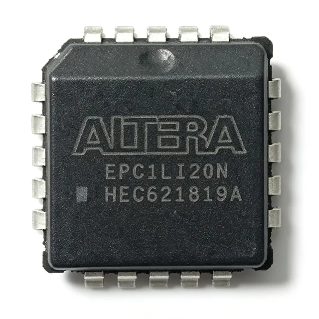
EPC1LI20N - 1Mb OTP FPGA Configuration PROM | Altera
MPN: EPC1LI20N ⚠ Last Time Buy| Qty | Unit Price | Extended |
|---|---|---|
| 1 | $10.5 | $10.50 |
| 10 | $9.95 | $99.50 |
| 100 | $9.2 | $920.00 |
| 500 | $8.5 | $4,250.00 |
| 1,000 | $7.8 | $7,800.00 |
EPC1LI20N Overview
A configuration PROM is a non-volatile serial memory that stores the FPGA's bitstream and presents it to the FPGA's configuration controller on power-up. In the Altera taxonomy, the EPC1 family sits at the entry tier: a single-device, OTP solution for LUT-based FPGAs such as the Cyclone, FLEX 10K, and APEX families. EPC1 devices are programmed once with the Quartus / MAX+PLUS II software flow and then permanently drive nCONFIG, DCLK, and DATA0 lines during every subsequent FPGA configuration.
Key specifications include a 1 Mb (1,048,576-bit) memory capacity, JTAG-compliant IEEE 1149.1 boundary-scan interface for in-system programming, a low-pin-count serial interface that minimizes FPGA pin usage during configuration, and programmable compression support that reduces configuration file size by 30-55%. The PLCC-20 footprint is the same J-lead package used across the entire EPC1 / EPC2 family, allowing board designers to migrate between OTP and flash-backed variants without PCB rework.
The EPC1 architecture uses an internal oscillator and state machine to implement Altera's proprietary serial configuration protocol, automatically detecting the target FPGA density and clocking the bitstream without external glue logic. This makes it ideal for cost-sensitive, single-FPGA designs where board space and BOM count matter more than field-upgradability.
Typical applications include factory-programmed FPGA configuration in industrial controllers, telecom line cards, and instrumentation where the bitstream is fixed for the product's lifetime. Engineers commonly pair the EPC1LI20N with Altera Cyclone II / III, FLEX 10KE, and ACEX 1K devices.
When designing with the EPC1LI20N, note that the device is OTP - any bitstream revision requires physical replacement. Reserve the JTAG pins on the FPGA so the EPC1 can be programmed through the FPGA's JTAG chain in production.
This page synthesizes distributor stock, parametric cross-references, and application guidance specific to the EPC1LI20N's 20-PLCC OTP configuration role - information not assembled in any single distributor listing.
Drop-in alternatives for EPC1LI20N — same package, pin-to-pin compatible. Different-package parts requiring PCB rework are excluded.
Variants in this series
Same-series models that are drop-in compatible with EPC1LI20N (same form factor and footprint) — differing in Memory Size, Mounting Type, Memory Type, Interface, Package.
Quick Comparison Tool — Select alternative parts for side-by-side comparison:
EPC1LI20
✓ In Stock
$8.5 / Unit
View Datasheet →EPC1LC20N
✓ In Stock
$8.4 / Unit
View Datasheet →EPC2LI20N
✓ In Stock
$5.1 / Unit
View Datasheet →EPC1LC20HEC
✓ In Stock
$9.6 / Unit
View Datasheet →EPC1LC20CEC
✓ In Stock
$7.2 / Unit
View Datasheet →EPC1441LC20N
✓ In Stock
$7.95 / Unit
View Datasheet →EPC1LI20N Maximum Ratings & Electrical Characteristics
| Memory Type | OTP Configuration PROM (One-Time Programmable) |
| Memory Size | 1 Mbit (1,048,576 bits) |
| Interface Type | Serial (Altera proprietary configuration protocol) |
| Package / Case | 20-LCC (J-Lead), PLCC-20 |
| Package Dimensions | 9 mm x 9 mm (PLCC-20 J-lead) |
| Supply Voltage - VCCINT | 3.0 V to 3.6 V |
| Supply Voltage - VCCIO | 4.5 V to 5.5 V |
| Operating Temperature | -40C to +85C (Industrial) |
| JTAG / Boundary Scan | IEEE 1149.1 compliant (for programming) |
| Programmable Compression | Yes (reduces bitstream 30-55%) |
| Mounting Type | Surface Mount (PLCC socket or solder) |
| Packaging | Tube |
| Lead Finish | Matte Sn (per JEDEC J-STD-020) |
| RoHS Status | Compliant |
| Target FPGA Families | Cyclone, FLEX 10K, APEX, ACEX 1K (LUT-based) |
EPC1LI20N Pin Configuration
| Pin 1 | VCC — Core supply voltage (3.0-3.6 V) |
| Pin 2 | nCS — Chip select (active low) |
| Pin 3 | DCLK — Configuration clock to FPGA |
| Pin 4 | DATA — Serial configuration data output |
| Pin 5 | nCONFIG — Configuration control (active low) |
| Pin 6 | nSTATUS — Configuration status (active low) |
| Pin 7 | CONF_DONE — Configuration done indicator |
| Pin 8 | GND — Ground |
| Pin 9 | OE — Output enable |
| Pin 10 | nCE — Chip enable (active low) |
| Pin 11 | MODE — Mode select |
| Pin 12 | VCCIO — I/O supply voltage (4.5-5.5 V) |
| Pin 13 | GND — Ground |
| Pin 14 | NC — Not connected (per datasheet) |
| Pin 15 | NC — Not connected (per datasheet) |
| Pin 16 | NC — Not connected (per datasheet) |
| Pin 17 | TDI — JTAG Test Data In (IEEE 1149.1) |
| Pin 18 | TDO — JTAG Test Data Out |
| Pin 19 | TMS — JTAG Test Mode Select |
| Pin 20 | TCK — JTAG Test Clock |
Typical Applications
EPC1LI20N is suitable for 6 applications: Cyclone FPGA Factory Configuration, FLEX 10K Industrial Controller Bitstream Storage, Telecom Line Card Configuration, Test & Measurement Instrument FPGA Boot, Mil/Aero Single-Board Computer FPGA Companion, Educational / Development Board FPGA Bitstream.
Cyclone FPGA Factory Configuration
The EPC1LI20N is a textbook fit for factory-programmed Cyclone (EP1C3, EP1C6, EP1C12) and Cyclone II (EP2C5/8/20) designs where the bitstream is fixed for the product's lifetime. With 1 Mbit of OTP storage and Altera's serial configuration protocol, it can load any Cyclone I/II bitstream without external glue logic, requiring only four FPGA pins (nCONFIG, DCLK, DATA0, CONF_DONE). At a 10.50 USD price point as of 2026-09-11 it is the lowest-cost configuration memory option in Altera's portfolio. The 20-PLCC socket allows field replacement during pilot runs, while in production the device can be hand-soldered or socketed. Designers should reserve FPGA JTAG pins so the EPC1 can be programmed through the JTAG chain in-circuit during manufacturing, avoiding a separate standalone programmer.
Recommended
FLEX 10K Industrial Controller Bitstream Storage
Legacy FLEX 10K and FLEX 10KE industrial controllers commonly use the EPC1LI20N as the boot configuration memory because the part implements Altera's original serial configuration protocol that FLEX 10K natively supports. The -40C to +85C industrial temperature range matches factory-floor and outdoor cabinet environments. The dual-rail 3.3 V/5 V supply lets the EPC1 interface directly to 5 V FLEX 10K I/O without level shifters, a significant advantage over single-rail PROMs. As a 1 Mbit OTP, it is suitable for FLEX 10K designs whose compressed bitstream fits below 1 Mb - typically EPF10K30, EPF10K50, and smaller. Designers migrating older FLEX 10K boards should verify bitstream size in MAX+PLUS II before committing to EPC1, since EPF10K100 and larger may exceed 1 Mb compressed.
Recommended
Telecom Line Card Configuration
In telecom line-card designs where the FPGA bitstream is locked at card calibration (per-line equalization coefficients etc.), the EPC1LI20N's OTP behavior is acceptable and even desirable - it prevents accidental in-field reprogramming that could cause regulatory or security issues. The 20-PLCC J-lead package withstands the higher vibration and thermal-cycling stresses of telecom shelves, and the -40C to +85C industrial temperature range covers central-office and outdoor-cabinet environments. The 1 Mb capacity fits the bitstream of small-to-mid density APEX 20K and ACEX 1K devices used for line-card glue logic. As of 2026-09-11, the EPC1LI20N's last-time-buy status means telecom OEMs planning new line-card platforms should qualify the EPC2LI20N (same footprint, field-reprogrammable) or migrate to a modern configuration scheme.
Recommended
Test & Measurement Instrument FPGA Boot
Bench-top and rack-mount test instruments (oscilloscopes, signal generators, protocol analyzers) often embed an Altera FPGA for DSP and timing, and the EPC1LI20N serves as a compact, low-cost OTP configuration memory. Because the instrument firmware is rarely field-upgraded through the FPGA path (it goes through a separate microcontroller), OTP behavior is acceptable. The 20-PLCC package fits the dense instrument mainboards where vertical PLCC sockets save board area versus SOIC alternatives. The 3.3 V/5 V dual supply aligns with the legacy 5 V system rails common in mixed-signal instruments. The IEEE 1149.1 JTAG interface allows production programming through the instrument's existing JTAG test access port without a separate programmer fixture.
Recommended
Mil/Aero Single-Board Computer FPGA Companion
Defense and aerospace single-board computers (SBCs) frequently use Altera ACEX or APEX FPGAs as bus-interface and signal-conditioning glue, with the EPC1LI20N providing locked bitstream storage. The industrial -40C to +85C temperature range is acceptable for many Mil/Aero ground systems (though not full -55C to +125C Mil-PRF requirements). The 20-PLCC through-hole-compatible J-lead package offers robust mechanical attachment under vibration, exceeding the reliability of fine-pitch QFN PROMs. Because Mil/Aero programs have long qualification cycles and parts must be traceable, distributors showing EPC1LI20N stock with date codes need to be vetted for AS6081 counterfeit-mitigation compliance.
Recommended
Educational / Development Board FPGA Bitstream
University FPGA teaching labs and Altera/Intel-developed education boards often include an EPC1LI20N (or its socket-compatible EPC2LI20N) to demonstrate the FPGA configuration process. Because student designs are rebuilt every semester, the OTP nature of EPC1 makes sense only if each design is pre-baked before the lab, but for the same reason many educational boards use EPC2LI20N instead. The 20-PLCC socketed footprint lets students physically swap between a pre-programmed EPC1 (for stable demo designs) and an EPC2 (for in-lab reprogramming). The low 10.50 USD single-piece price as of 2026-09-11 makes EPC1LI20N acceptable for one-off teaching kits, although boards shipping in 2026 should consider whether to migrate to a modern MAX II or MAX V CPLD-based configuration scheme.
Recommended
Recommended Products Summary
Engineering reference data for EPC1LI20N — comparison, design guidance, and compliance information.
Selection Guide
Comparison with Alternatives
| Parameter | This Product | EPC1LI20 | EPC1LC20N | EPC2LI20N | EPC1LC20HEC | EPC1LC20CEC | EPC1441LC20N |
|---|---|---|---|---|---|---|---|
| Brand | Altera (Intel) | Altera (Intel) | Altera (Intel) | Altera (Intel) | Altera (Intel) | Altera (Intel) | Altera (Intel) |
| Package | 20-PLCC (J-Lead), 9x9 mm | 20-PLCC (J-Lead) - same | 20-PLCC (J-Lead) - same | 20-PLCC (J-Lead) - same | 20-PLCC (J-Lead) - same | 20-PLCC (J-Lead) - same | 20-PLCC (J-Lead) - same |
| Memory Size | 1 Mbit | 1 Mbit | 1 Mbit | 2 Mbit | 1 Mbit | 1 Mbit | 1 Mbit (older EPC1441 family) |
| Memory Type | OTP (one-time programmable) | OTP | OTP | Flash (reprogrammable) | OTP | OTP | OTP (older family) |
| Supply Voltage (VCCINT) | 3.0 - 3.6 V | 3.0 - 3.6 V | 3.0 - 3.6 V | 3.0 - 3.6 V | 3.0 - 3.6 V | 3.0 - 3.6 V | 3.0 - 3.6 V |
| Operating Temperature | -40C to +85C | -40C to +85C | -40C to +85C | -40C to +85C | -40C to +85C | -40C to +85C | -40C to +85C |
| JTAG / Boundary Scan | Yes (IEEE 1149.1, programming only) | Yes (programming only) | Yes (programming only) | Yes (programming + in-system update) | Yes (programming only) | Yes (programming only) | Yes (programming only) |
| Lifecycle Status (2026) | Last-time-buy | Last-time-buy | Last-time-buy | Last-time-buy / NRND | Last-time-buy | Last-time-buy | Obsolete |
Key Differentiators
- Smallest, lowest-cost Altera configuration PROM (vs EPC2LI20N)
- Original Altera serial configuration protocol (vs EPC1441LC20N)
- Dual-rail 3.3 V/5 V supply supports legacy 5 V FPGAs directly (vs EPC1LI20 (SnPb lead finish))
Design Notes
The EPC1LI20N requires two separate supply rails: VCCINT (3.0-3.6 V, typically 3.3 V) for the core logic and VCCIO (4.5-5.5 V, typically 5.0 V) for the FPGA-facing I/O. Per the Altera datasheet, VCCIO must be present whenever the PROM is driving the configuration bus; powering VCCINT without VCCIO can latch up I/O structures. Decouple each supply with a 100 nF ceramic capacitor placed within 5 mm of the corresponding pin, plus a 10 uF bulk capacitor on the board's 3.3 V and 5 V rails. Estimated: at idle, the EPC1 draws under 50 mA combined; during configuration burst it draws up to ~100 mA on VCCINT, so the regulator should have at least 200 mA headroom.
Mount the EPC1LI20N in a 20-PLCC socket (e.g., 3M 8200-series or equivalent) rather than soldering directly if the bitstream may change during pilot runs. The J-lead footprint tolerates standard J-STD-020 reflow profiles (245C peak for SnPb or 260C peak for lead-free) when direct soldering is preferred for production. Per Altera layout guidelines, route DCLK as a short (<50 mm) trace and place a 33 ohm series-termination resistor if the trace exceeds 25 mm, to limit ringing. Keep DATA away from switching power converter edges by at least 3 mm to avoid coupling during configuration when the FPGA is in high-impedance mode.
Three pitfalls trip up first-time users: (1) The 'LI' suffix is required for industrial-temperature operation; do not substitute commercial-temperature variants in outdoor or factory-floor designs. (2) The OTP nature means every engineering bitstream change requires physical PROM replacement or use of a separate programmer - plan pilot runs with socketed EPC1 or migrate to EPC2LI20N for in-system reprogram. (3) The EPC1 does not generate DCLK for the FPGA when nCONFIG is high; ensure the FPGA's internal oscillator or an external clock is configured properly, or the configuration bus will idle. Verify CONF_DONE goes high within 100 ms after nCONFIG release, otherwise the FPGA has failed to configure.
Compliance Information
RoHS compliant per Altera/Intel product declaration. The 'N' suffix indicates lead-free matte-Sn finish (JEDEC J-STD-020). Industrial temperature -40C to +85C; not AEC-Q100 qualified for automotive. REACH compliance follows standard Altera declaration.




