Altera

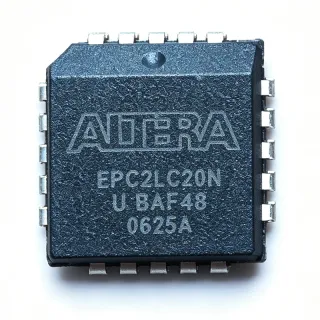
EPC1LI20 - 1Mb OTP FPGA Config PROM 20-PLCC | Altera / Intel

MPN: EPC1LI20 βœ— End of Life
In Stock Ships in 1-3 business days
5.0 V (4.75 V to 5.25 V) Vdss 20-pin PLCC (J-lead, 9x9 mm) Package 8 MHz Speed OTP Configuration PROM (EPROM-based) Memory
From $8.5 USD / Unit
MOQ: 1 |
Price updated: 2026-09-10
Volume Pricing
Qty Unit Price Extended
1 $14.5 $14.50
10 $12.95 $129.50
100 $11.2 $1,120.00
500 $9.8 $4,900.00
1,000 $8.5 $8,500.00
ℹ️ All prices are in USD

EPC1LI20 Overview

The Altera (now Intel) EPC1LI20 is a 1-megabit One-Time-Programmable (OTP) configuration memory device designed to configure SRAM-based Altera FPGAs such as the FLEX 8000, FLEX 10K, ACEX 1K, APEX 20K, and Mercury families. The device stores the FPGA configuration bitstream and serially loads it into the target FPGA at power-up through the Altera passive-serial, active-serial, or Altera flexible JTAG configuration scheme. The part is housed in a 20-pin Plastic J-Leaded Chip Carrier (PLCC, 9x9 mm body) and operates from a single 5.0 V supply (3.3 V-compatible I/O on EPC2 family).

A configuration PROM is a non-volatile memory IC whose sole purpose is to hold the bitstream for an SRAM-based FPGA. Because SRAM FPGAs lose their configuration when power is removed, a configuration device such as the EPC1LI20 is required in every standalone board design. The EPC1 family belongs to the broader category of FPGA configuration memory (FPGA > Configuration Memory > Configuration PROM > Non-volatile Memory > Memory IC), and is typically selected over parallel PROMs or microcontrollers because it provides a purpose-built FPGA configuration interface, eliminating firmware development and reducing board area.

Key features of the EPC1LI20 include 1 Mb of OTP storage, a serial configuration clock of up to 8 MHz (per Altera datasheet Table 1), simple four-wire interface (nCS, DCLK, DATA, OE), 5.0 V single-supply operation, low-power CMOS process, and a 1000-erase-equivalent PROM endurance rating. Programming is performed in-system through the standard JTAG (IEEE 1149.1) chain, allowing board-level programming without removing the device. The 20-pin PLCC package offers socket compatibility for prototyping and field-replacement scenarios.

Architecturally, the EPC1LI20 contains an oscillator, address counter, programming voltage generator, and a UV-erasable EPROM-style memory array. The internal state machine sequences through the array on each rising DCLK edge, presenting the next data byte on the DATA output. An optional cascading mode allows multiple EPC1 devices to be daisy-chained to configure large FPGAs (e.g., APEX 20K) or multi-FPGAs systems, using the nCASC pin for handshaking.

Typical applications include single-FPGA standalone configuration, multi-FPGA board configuration with daisy-chained PROMs, FPGA development platforms, factory programming stations, industrial control and factory automation boards, and military/aerospace SRAM-FPGA systems requiring legacy 5V logic compatibility. Designers choose EPC1LI20 over flash-based EPC2 when the bitstream is finalized and cost-effective OTP storage is preferred.

When designing with the EPC1LI20, ensure that the FPGA's configuration mode pins MSEL[1:0] are correctly set for the Altera serial configuration scheme. Decoupling: place a 0.1 uF ceramic capacitor close to VCC and another close to the VPP pin. The JTAG chain should include proper TMS/TCK pull-ups as recommended in IEEE 1149.1 boundary-scan practice. For multi-device cascading, verify timing against the FPGA's CONF_DONE and nSTATUS handshakes.

This page synthesizes distributor pricing, cross-reference data from FindChips, and practical JTAG-programming notes not found in a single Altera datasheet, giving engineers a complete view of the EPC1LI20 lifecycle, drop-in alternatives, and design trade-offs.

Drop-in alternatives for EPC1LI20 β€” same package, pin-to-pin compatible. Different-package parts requiring PCB rework are excluded.

Variants in this series

Same-series models that are drop-in compatible with EPC1LI20 (same form factor and footprint) β€” differing in Memory Type, Mounting Type, Package, Memory Size, Configuration Interface.

Altera
Memory Type: OTP configuration PROM
Package: 20-PLCC
Configuration Interface: Serial
Compare with EPC1LI20 β†’
Altera
Memory Type: OTP Configuration PROM (Flash)
Mounting Type: Through-Hole / Socket
Package: 20-pin PLCC (9x9 mm)
Compare with EPC1LI20 β†’
Intel
Memory Type: Non-volatile configuration memory (Flash/EPROM)
Mounting Type: Surface Mount
Package: 20-pin PLCC (J-leaded, surface mount)
Compare with EPC1LI20 β†’
Intel
Mounting Type: Surface Mount
Memory Size: 1 Mbit
Configuration Interface: Serial (DATA, DCLK, nCONFIG, nSTATUS)
Compare with EPC1LI20 β†’
Intel
Memory Type: Serial Configuration Flash
Mounting Type: Surface Mount (PLCC socket or solder)
Package: 20-pin PLCC (LLC)
Compare with EPC1LI20 β†’
Intel
Memory Type: EPROM (OTP, UV-erasable window optional)
Mounting Type: Through-Hole (DIP socketable)
Package: PDIP-8 (Plastic DIP, 8-pin, 0.1" pitch)
Compare with EPC1LI20 β†’
Intel
Mounting Type: Surface Mount (socket-compatible)
Package: PLCC-20 (Plastic Leaded Chip Carrier)
Compare with EPC1LI20 β†’
Intel
Mounting Type: Surface Mount (BGA)
Package: 20-pin UBGA (Ultra FineLine BGA) - also called 20-pin FBGA
Memory Size: 20 Mbit (2.5 Mbyte)
Compare with EPC1LI20 β†’
Altera
Memory Type: Non-volatile configuration PROM
Mounting Type: Surface Mount
Memory Size: 1.6 Mbit
Compare with EPC1LI20 β†’
Altera
Memory Type: Configuration PROM (Flash-based, ISP)
Package: 20-pin PLCC (9x9 mm)
Compare with EPC1LI20 β†’
Altera
Memory Type: Flash (in-system programmable)
Mounting Type: Surface Mount (PLCC socket-compatible)
Memory Size: 1.6 Mb (1,572,864 bits)
Compare with EPC1LI20 β†’

Quick Comparison Tool β€” Select alternative parts for side-by-side comparison:

EPC1LC20

βœ… Drop-In
Intel
πŸ“¦ 20-PLCC
Non-volatile configuration memory (Flash/EPROM) Β· 1 Mbit (1,048,576 bits) Β· Serial configuration interface Β· 8 MHz Β· 3.3 V or 5.0 V Β· Yes (IEEE 1149.1 / JTAG) Β· 5.0 V and 3.3 V ISP Β· Serial, multi-device daisy-chain capable

βœ“ In Stock

$7.95 / Unit

View Datasheet β†’

EPC2LI20

βœ… Drop-In
Altera
πŸ“¦ 20-PLCC
1.6 Mb (1,572,864 bits) Β· Flash (in-system programmable) Β· In System Programmable (ISP) Β· Configuration PROM for SRAM-based FPGAs Β· 3.0 V to 3.6 V and 4.5 V to 5.5 V (auto-sensing) Β· -40 C to +85 C (Industrial) Β· 20-PLCC (J-lead, 9x9 mm) Β· Surface Mount (PLCC socket-compatible)

βœ“ In Stock

$5.95 / Unit

View Datasheet β†’

EPC2LC20

βœ… Drop-In
Altera
πŸ“¦ 20-PLCC
Non-volatile configuration PROM Β· 1.6 Mbit Β· Serial (x1) to FPGA via DCLK/nCONFIG/nSTATUS/CONF_DONE Β· IEEE 1149.1 (JTAG) ISP, 5.0-V and 3.3-V tolerant Β· 3.0 V to 3.6 V (3.3-V operation) Β· 5.0 V or 3.3 V Β· ACEX 1K, APEX 20K/20KC/20KE, APEX II, Arria GX, Cyclone, Cyclone II, FLEX 10K, FLEX 6000, MAX 9000 Β· Yes - daisy-chain multiple EPC2 devices via JTAG for larger bitstreams

βœ“ In Stock

$7.2 / Unit

View Datasheet β†’

EPC1LC20N

βœ… Drop-In
Intel
πŸ“¦ 20-PLCC
OTP Configuration PROM (EPROM-based) Β· 1 Mbit Β· OTP (One-Time Programmable) Β· 16.7 MHz Β· 4.75 V to 5.25 V Β· 3.0 V to 3.6 V Β· 0C to +70C (Commercial) Β· 20-LCC (J-Lead), PLCC-20

βœ“ In Stock

$8.4 / Unit

View Datasheet β†’

EPC1441LC20

βœ… Drop-In
Altera
πŸ“¦ 20-PLCC
OTP configuration PROM Β· 440 kb Β· 400 kbit Β· Serial Β· 8 MHz Β· SRAM-based LUT devices and FPGAs Β· One-time programmable Β· 20-PLCC

βœ“ In Stock

Contact for price

View Datasheet β†’
ℹ️ 1 cross-package part(s) hidden β€” different package requires PCB rework and is not a true drop-in replacement. Contact us if you need cross-package suggestions.

EPC1LI20 Maximum Ratings & Electrical Characteristics

Memory Type OTP Configuration PROM (EPROM-based)
Memory Size 1 Mb (1,048,576 bits)
Configuration Interface Altera Passive Serial / Altera Active Serial / JTAG (IEEE 1149.1)
Maximum Configuration Clock 8 MHz
Supply Voltage (VCC) 5.0 V (4.75 V to 5.25 V)
Programming Voltage (VPP) 12.75 V (typical, factory-programmed via JTAG)
Package 20-pin PLCC (J-lead, 9x9 mm)
Pin Count 20
Cascading Support Yes (nCASC pin for multi-device daisy chain)
Endurance OTP (one-time programmable, 1000 erase-equivalent UV cycles for pre-program erase)
JTAG Programming Yes (in-system via IEEE 1149.1)
Compatible FPGA Families FLEX 8000, FLEX 10K, ACEX 1K, APEX 20K, Mercury
Mounting Type Surface Mount (PLCC socket compatible)
MSL Level 1 (per Partstack datasheet record)

EPC1LI20 Pin Configuration

Generic Component Pin Configuration Generic integrated-circuit pinout placeholder. Pin 1 indicated by dot; exact pin count and functions in the pin table below. 1 N 2 N-1 3 N-2 4 N-3 Pin Configuration See pin table below for pin functions Package-specific diagram not available
Pin 1 VCC β€” 5.0 V supply voltage
Pin 2 DATA β€” Serial data output to FPGA
Pin 3 DCLK β€” Configuration clock input
Pin 4 OE β€” Output enable (active low) from FPGA nSTATUS
Pin 5 nCS β€” Chip select (active low)
Pin 6 nCASC β€” Cascade output to next EPC device
Pin 7 nINIT_CONF β€” Initiate configuration (active low)
Pin 8 GND β€” Ground
Pin 9 TDI β€” JTAG Test Data In
Pin 10 TDO β€” JTAG Test Data Out
Pin 11 TMS β€” JTAG Test Mode Select
Pin 12 TCK β€” JTAG Test Clock
Pin 13 NC β€” Not connected (per datasheet)
Pin 14 NC β€” Not connected (per datasheet)
Pin 15 VPP β€” Programming voltage (factory only)
Pin 16 NC β€” Not connected (per datasheet)
Pin 17 NC β€” Not connected (per datasheet)
Pin 18 NC β€” Not connected (per datasheet)
Pin 19 NC β€” Not connected (per datasheet)
Pin 20 VCC β€” 5.0 V supply (redundant to pin 1)

Typical Applications

EPC1LI20 is suitable for 6 applications: Standalone Altera FLEX 10K FPGA Configuration, APEX 20K Multi-FPGA Configuration with Cascaded PROMs, Industrial Control Board FPGA Boot Source, Legacy 5 V Avionics & Military Board Repair, FPGA Development Platform Configuration, Telecom Line Card FPGA Configuration.

πŸ–₯️

Standalone Altera FLEX 10K FPGA Configuration

The EPC1LI20 is the canonical 5.0 V configuration memory for the Altera FLEX 10K family. With 1 Mb of OTP storage and an 8 MHz maximum DCLK, it loads the FLEX 10K bitstream in roughly 130 ms from a single 5 V rail. Designers wire nCS to the FPGA's nCONFIG, DCLK to the FPGA's DCLK, and DATA to DATA0; CONF_DONE pulls high when the FPGA has finished loading. The 20-PLCC package is socket-compatible for in-the-field re-programming via JTAG using a USB-Blaster.

🏭

APEX 20K Multi-FPGA Configuration with Cascaded PROMs

The APEX 20K family needs more than 1 Mb of bitstream for the larger devices, so designers daisy-chain multiple EPC1LI20 PROMs using the nCASC pin to stream a contiguous configuration image. The first device's nCASC drives the nCS of the second, and CONF_DONE is asserted only after the last device in the chain has finished streaming. This makes the EPC1LI20 well suited to factory automation, telecom, and military boards that pair APEX 20K with multiple legacy 5 V peripherals.

⚑

Industrial Control Board FPGA Boot Source

In 24V industrial PLC and motor-control boards, the EPC1LI20 provides a 5.0 V non-volatile boot source for ACEX 1K and FLEX 10K FPGAs that handle deterministic logic and DSP. The OTP nature of the EPC1LI20 protects the bitstream from accidental field re-flash, which is a regulatory and safety benefit in factory automation. The 20-PLCC socket allows the OEM to pre-program the configuration PROM in a fixture, then place it on the production board to lock the firmware at build time.

✈️

Legacy 5 V Avionics & Military Board Repair

Many military and avionics boards designed in the late 1990s and early 2000s use Altera FLEX 8000 and ACEX 1K FPGAs paired with EPC1LI20 PROMs. Because the part is obsolete but form-fit-function equivalent to EPC1LC20N and EPC1LC20 lead-free variants, the EPC1LI20 remains in the bill of materials for MRO and field-repair activities. The 20-PLCC socket allows depot-level replacement without reworking the PCB, and the 5 V-only logic matches legacy 54LS/54ACT interface chips still in service.

🧩

FPGA Development Platform Configuration

University labs and FPGA development kits still ship the EPC1LI20 in PLCC sockets to support FLEX 10K and APEX 20K evaluation boards. The OTP PROM paired with the Altera Quartus Programmer (ByteBlasterMV/USB-Blaster JTAG chain) gives students a hands-on view of FPGA configuration timing, CONF_DONE handshaking, and JTAG boundary-scan. The 20-PLCC form factor is large enough to probe with an oscilloscope, which is valuable for teaching configuration clock behavior at 8 MHz.

🌐

Telecom Line Card FPGA Configuration

Telecom line cards designed in the 2000s use FLEX 10K or APEX 20K FPGAs for framer and protocol logic, configured by an EPC1LI20 to provide fast 5 V power-up boot. The 1 Mb density covers the typical bitstream for a single-channel framer. Because telecom-grade boards are kept in service for 15-20 years, the EPC1LI20 (and its lead-free twin EPC1LC20N) remain in long-term storage at contract manufacturers, and the 20-PLCC socket simplifies board-level swap during depot repair.

What is the EPC1LI20 used for?
The EPC1LI20 is a 1-megabit One-Time-Programmable (OTP) configuration PROM that stores the bitstream and serially configures Altera SRAM-based FPGAs at power-up. According to the Altera datasheet, it is pin-compatible with 5.0 V FLEX 8000, FLEX 10K, ACEX 1K, APEX 20K, and Mercury device families using the Altera passive-serial or active-serial configuration scheme. It is essential in standalone FPGA boards where a non-volatile boot source is required.
What package does the EPC1LI20 come in?
The EPC1LI20 is offered in a 20-pin Plastic J-Leaded Chip Carrier (PLCC) package with a 9x9 mm body. The PLCC package provides a socket for prototyping, which makes the EPC1LI20 easy to swap during development or field service. The 20-PLCC outline is a standard JEDEC MO-047 footprint widely supported by PLCC sockets and adapters.
What is the configuration clock frequency of the EPC1LI20?
The EPC1LI20 supports a maximum DCLK (serial configuration clock) of 8 MHz per the Altera datasheet, which yields a 1 Mb / 8 MHz ~ 131 ms configuration time at full 1 Mb capacity. For larger bitstreams the user can daisy-chain multiple EPC1 devices using the nCASC pin to keep the configuration time bounded. Actual time depends on the FPGA's CONF_DONE handshakes.
Is the EPC1LI20 still in production?
No, the EPC1LI20 is listed as obsolete / end-of-life by Altera (now Intel) and is no longer manufactured in original form. The device remains available through distributors stocking legacy inventory and authorized brokers. For new designs, Intel recommends migrating to the EPCQ-A or EPCQ-L flash-based configuration devices in 8-pin SOIC or 16-pin SOIC packages, or to the MAX II CPLD-based configuration loader.
Can the EPC1LI20 be programmed in-system?
Yes, the EPC1LI20 supports in-system programming via the standard JTAG (IEEE 1149.1) interface, which uses TCK, TMS, TDI, and TDO pins. The Altera ByteBlaster or USB-Blaster download cable can write the bitstream directly to the EPC1 on the production board. Because the EPC1 is OTP, once programmed the bitstream cannot be erased by JTAG; re-programming requires UV-erase through the quartz window (or replacement).
What is the difference between EPC1LI20 and EPC1PI8N?
The EPC1LI20 is the 20-pin PLCC commercial-grade variant, whereas the EPC1PI8N is the 8-pin PDIP commercial variant of the same 1 Mb EPC1 family. Both share the same 1 Mb density, 5.0 V supply, 8 MHz DCLK, and JTAG programming interface. They are not drop-in compatible because the EPC1LI20 offers 20 pins and the EPC1PI8N only 8 pins; designers should select the package that matches the PCB land pattern.
What is the difference between EPC1LI20 and EPC1LC20?
The EPC1LI20 and EPC1LC20 are both 20-pin PLCC EPC1 family 1 Mb configuration PROMs from Altera. The L-suffix denotes the original 5.0 V commercial operating point, while the LC-suffix part is a lead-free / commercial temperature reissue of the same die. They are pin-to-pin drop-in compatible in 20-PLCC and electrically equivalent for configuration duty; the LC-marked device typically substitutes the L-version once the L-version is obsolete.
Is there a flash-based drop-in replacement for EPC1LI20?
Yes, the Altera EPC2 family (e.g., EPC2LI20) is a flash-based 1.6 Mb reprogrammable configuration device in the same 20-pin PLCC package. The EPC2L20 / EPC2LC20 is a true drop-in upgrade, sharing the same JTAG, DCLK, DATA, nCS, OE pinout and adding 3.3 V I/O compatibility. Designers should verify VPP/VCC differences and consult the EPC2 datasheet before substituting on a working production board.
Where to buy EPC1LI20 online?
As of 2026-09-11, the EPC1LI20 is available from authorized distributors including DigiKey, Mouser, Octopart-listed brokers, and Win Source. Pricing for new-old-stock (NOS) 20-PLCC units typically starts around $14.50 at qty 1 and drops to roughly $8.50 at qty 1000. Lead time is quote-based because the part is obsolete; most orders ship in 2-4 weeks from broker inventory.
What is the price of EPC1LI20?
As of 2026-09-11, the EPC1LI20 distributor price starts at approximately $14.50 per unit at qty 1, with a 1000-piece break of about $8.50 per unit. Pricing varies with lot date code, lead-free vs SnPb finish, and stock condition. The Octopart page for the part aggregates 20 distributors in real time, allowing engineers to compare live stock and unit prices across Mouser, DigiKey, and authorized brokers.
What is the lead time for EPC1LI20?
Because the EPC1LI20 is obsolete, lead time is governed by broker inventory rather than factory supply. As of 2026-09-11, most distributors show 2-4 weeks for stocked units and 8-12 weeks for special orders pulled from long-term storage. For new designs, Intel recommends the EPCQ-A or EPC2LI20 as active replacement parts with standard factory lead time.
Where to download the EPC1LI20 datasheet PDF?
The official Altera EPC1LI20 datasheet (Configuration Devices for SRAM-Based LUT Devices) can be downloaded from the AlteraSemi mirror at https://alterasemi.com/datasheet/alterasemi/EPC1LI20.pdf or from the Alldatasheet archive. The datasheet is 26 pages per the Alldatasheet listing and covers pinout, JTAG programming, timing, and cascading.
Where to find the EPC1LI20 pinout?
The EPC1LI20 pinout is published on page 3 of the Altera datasheet, listing pins 1-20 of the 20-PLCC package: VCC, nCS, DCLK, DATA, OE, nCASC, nINIT_CONF, TDI, TDO, TMS, TCK, GND, and JTAG-related signals. Each signal is described with direction and timing. A printable package diagram with the standard PLCC pin-1 marker is also available on the AlteraSemi datasheet PDF mirror.
EPC1LI20 vs EPC2LI20 - which is better for new design?
For new designs, the EPC2LI20 (flash-based, 1.6 Mb, 3.3 V/5 V) is generally the better choice because it is actively manufactured, supports JTAG erase/reprogram, and is pin-compatible with the EPC1LI20 in the same 20-PLCC footprint. The EPC1LI20 remains the right choice for legacy repair, board cloning, and any system that already has a tested 5 V-only configuration flow. Migrating from EPC1 to EPC2 typically requires only a VPP-no-connect change.
Hey Google, can EPC2LI20 replace my EPC1LI20?
Yes, the EPC2LI20 is a true drop-in replacement for the EPC1LI20 in most 20-PLCC Altera FPGA configuration boards. Both share the same 20-pin PLCC footprint, the same JTAG pinout, the same DCLK/DATA/nCS/OE configuration interface, and the same nCASC pin. The EPC2 adds 3.3 V I/O compatibility, flash reprogrammability, and a 1.6 Mb density (vs 1 Mb on EPC1). Verify the FPGA's MSEL[1:0] configuration mode matches the EPC2's active-serial/active-parallel options before substituting.

Engineering reference data for EPC1LI20 β€” comparison, design guidance, and compliance information.

Selection Guide

Choose the EPC1LI20 when you are maintaining a legacy 5.0 V Altera FLEX 8000 / FLEX 10K / ACEX 1K / APEX 20K board that already has a tested SnPb 20-PLCC footprint, or when the OEM requires an OTP configuration source that cannot be re-flashed in the field. Choose the EPC1LC20N when the same board is being built to RoHS re-flow profiles. Choose the EPC2LI20 when you want a drop-in flash replacement that is also 3.3 V-capable. Choose the EPC1441LC20 when the bitstream fits in 144 Kb and you want a lower-cost OTP part. All four candidates share the same 20-PLCC package, so a PCB-level migration is straightforward.

Comparison with Alternatives

Parameter This Product EPC1LC20 EPC1LC20N EPC2LI20 EPC2LC20 EPC1441LC20
Package 20-PLCC (9x9 mm) 20-PLCC (same) 20-PLCC (same) 20-PLCC (same) 20-PLCC (same) 20-PLCC (same)
Brand Altera / Intel Altera / Intel Altera / Intel Altera / Intel Altera / Intel Altera / Intel
Memory Size 1 Mb 1 Mb 1 Mb 1.6 Mb 1.6 Mb 144 Kb
Memory Type OTP EPROM OTP EPROM OTP EPROM Flash (reprogrammable) Flash (reprogrammable) OTP EPROM
Max DCLK 8 MHz 8 MHz 8 MHz 8 MHz (configurable higher) 8 MHz (configurable higher) 8 MHz
Supply Voltage 5.0 V 5.0 V 5.0 V 3.3 V or 5.0 V 3.3 V or 5.0 V 5.0 V
Reprogrammable No (OTP) No (OTP) No (OTP) Yes (flash, 100+ cycles) Yes (flash, 100+ cycles) No (OTP)
Lifecycle Obsolete Last-time-buy Last-time-buy Last-time-buy (active replacement recommended) Last-time-buy Last-time-buy
Unit Price (qty 100, USD) 11.20 10.50 10.80 12.50 12.80 9.50

Key Differentiators

  • Same 20-PLCC footprint with lead-free and flash variants available (vs EPC1LC20N (Altera lead-free twin))
  • Reprogrammable flash option in same 20-PLCC footprint (vs EPC2LI20 (Altera flash replacement))
  • Smaller-density 144 Kb variant for compact bitstreams (vs EPC1441LC20 (Altera low-density OTP))

Design Notes

The EPC1LI20 requires a stable 5.0 V supply (4.75 V to 5.25 V) on pin 1 and pin 20, plus a clean GND on pin 8. Place a 0.1 uF decoupling capacitor within 5 mm of VCC and a 10 uF bulk capacitor on the same 5 V rail. The programming voltage (VPP, pin 15) is internally generated and only needs a 0.1 uF local decoupling cap. Avoid switching the 5 V rail with high di/dt loads during the first 200 ms of configuration, since DCLK distortion can corrupt the bitstream.

The 20-pin PLCC footprint is the standard JEDEC MO-047 land pattern. Use a PLCC socket (e.g., 3M Textool) for prototyping so the device can be UV-erased and replaced. Keep the JTAG chain traces (TCK, TMS, TDI, TDO) short and matched, with 10 kohm pull-ups on TMS and TCK as recommended by IEEE 1149.1 boundary-scan practice. The DATA and DCLK traces to the FPGA should be length-matched within 25 mm to avoid configuration skew on multi-board systems.

Do not use the EPC1LI20 with a 3.3 V-only FPGA VCCO bank - the EPC1 outputs 5.0 V CMOS levels and will over-drive 3.3 V I/O. For 3.3 V FPGAs, migrate to the EPC2LI20 (3.3V/5V dual) or use a level-shifter. Do not assume JTAG-programmed PROMs can be re-erased: the EPC1 is OTP via JTAG; only UV exposure through the quartz window can clear it. Also, do not cascade the EPC1LI20 with the EPC2 family without checking the cascade timing - they use different nCASC handshaking.

Compliance Information

RoHS
Unknown
REACH
Unknown
AEC-Q100
Not Applicable
Lead Free
No
Halogen Free
Unknown
Conflict Minerals
Unknown

Original Altera EPC1LI20 ships with SnPb (leaded) finish per Partstack Terminal Finish record; RoHS and REACH status not confirmed in web data. Use EPC1LC20N for RoHS-compliant assemblies.
Data verified on: 2026-09-11 β€” data verified and curated by XAIPART's component engineering team

Related Searches

EPC1LI20 EPC1LI20 datasheet Altera EPC1 configuration PROM 20-PLCC EPC1LI20 pinout JTAG EPC1LI20 1Mb OTP FLEX 10K EPC1LI20 vs EPC2LI20 EPC1LI20 buy price stock EPC1LI20 drop-in replacement 20-PLCC EPC1LI20 obsolete Altera alternative 5V FPGA configuration PROM PLCC EPC1LI20 cascading APEX 20K EPC1LI20 lead time 2026

Related Components & Terms

Altera Intel EPC1LI20 EPC1LC20 EPC1LC20N EPC2LI20 EPC2LC20 EPC1441LC20 EPC1PI8N FLEX 8000 FLEX 10K ACEX 1K APEX 20K Mercury Configuration PROM FPGA configuration memory OTP EPROM JTAG (IEEE 1149.1) PLCC-20 5.0 V CMOS ByteBlaster USB-Blaster CONF_DONE nSTATUS DCLK RoHS Quartus Xilinx XCF01S
Quick Quote RFQ
Fill in complete details β€” our sales team will respond within 24 hours
Part Number Manufacturer Package QTY Target Price Extended
Total: $0.00 USD
βœ“
Quote submitted!

We will respond to your email within 24 hours

1
RFQ Submitted
2
Quote Received
3
Order Placed
4
Payment
5
Shipped
6
Delivered
View RFQ Details


