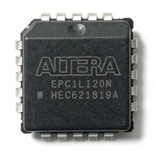
EPC1LC20N - 1Mb OTP FPGA Configuration PROM | Intel / Altera | PLCC-20
MPN: EPC1LC20N ✗ End of Life| Qty | Unit Price | Extended |
|---|---|---|
| 1 | $13.5 | $13.50 |
| 10 | $12.1 | $121.00 |
| 100 | $10.5 | $1,050.00 |
| 500 | $9.25 | $4,625.00 |
| 1,000 | $8.4 | $8,400.00 |
EPC1LC20N Overview
An FPGA configuration PROM is a non-volatile memory device that holds the bitstream which initializes an SRAM-based FPGA each time the system powers up or reinitializes. SRAM-based lookup-table (LUT) FPGAs, including members of the Altera FLEX, APEX, ACEX, and Mercury families, lose their configuration when power is removed, so an external boot memory is mandatory. The hierarchy is: configuration PROM -> boot memory -> FPGA companion chip -> programmable logic -> semiconductor. OTP variants such as the EPC1LC20N are typically used in production systems where the bitstream is finalized, while in-system programmable EPC2-series parts are preferred during development.
Key features of the EPC1LC20N include automatic CRC-based error detection, a daisy-chain capability for programming multiple devices in series, JTAG-friendly boundary-scan testability, and an open-drain CONF_DONE output. The part uses a simple 4-pin serial interface (DATA, DCLK, nCONFIG, nSTATUS) that is directly compatible with the FPP or PS configuration modes of Altera FPGAs, allowing board designers to drop the part into existing reference designs without glue logic.
Typical applications include Altera FLEX 10K, FLEX 6000, APEX 20K, ACEX 1K, and Mercury FPGA configuration stores, industrial controller bitstream backup, telecommunications line-card boot memory, and military / aerospace SRAM-FPGA initialization where field reprogrammability is not required.
When designing with this device, the EPC1LC20N should be paired with a 10 kohm pull-up on nSTATUS and a 10 kohm pull-up on CONF_DONE to guarantee valid logic levels during FPGA power-up sequencing.
Drop-in alternatives for EPC1LC20N — same package, pin-to-pin compatible. Different-package parts requiring PCB rework are excluded.
Variants in this series
Same-series models that are drop-in compatible with EPC1LC20N (same form factor and footprint) — differing in Package, Mounting Type, Memory Type, Operating Temperature, Compatible FPGA Families.
Quick Comparison Tool — Select alternative parts for side-by-side comparison:
EPC1LI20N
✅ Drop-In ⚠️ 参数待验证✓ In Stock
$7.8 / Unit
View Datasheet →EPC1LC20
✅ Drop-In ⚠️ 参数待验证✓ In Stock
$7.95 / Unit
View Datasheet →EPC2LC20N
✅ Drop-In ⚠️ 参数待验证✓ In Stock
$7.4 / Unit
View Datasheet →EPC2LI20N
✅ Drop-In ⚠️ 参数待验证✓ In Stock
$5.1 / Unit
View Datasheet →EPC1PI8N
✅ Drop-In ⚠️ 参数待验证✓ In Stock
$7.4 / Unit
View Datasheet →EPC144LC20
✅ Drop-In ⚠️ 参数待验证✓ In Stock
$7.1 / Unit
View Datasheet →EPC1LC20N Maximum Ratings & Electrical Characteristics
| Memory Type | OTP Configuration PROM (EPROM-based) |
| Memory Size | 1 Mbit |
| Programmable Type | OTP (One-Time Programmable) |
| Configuration Clock Frequency | 16.7 MHz |
| Supply Voltage - VCCINT | 4.75 V to 5.25 V |
| Supply Voltage - VCCIO | 3.0 V to 3.6 V |
| Operating Temperature | 0C to +70C (Commercial) |
| Package / Case | 20-LCC (J-Lead), PLCC-20 |
| Package Dimensions | 9 mm x 9 mm |
| Mounting Type | Surface Mount |
| Packaging | Tube |
| Configuration Interface | Serial (DATA, DCLK, nCONFIG, nSTATUS) |
| Supported FPGA Families | Altera FLEX, APEX, ACEX, Mercury |
EPC1LC20N Pin Configuration
| Pin 1 | VCC — 5 V core supply (4.75 V to 5.25 V) |
| Pin 2 | DATA — Serial data output to FPGA |
| Pin 3 | GND — Ground |
| Pin 4 | DCLK — Configuration clock input from FPGA |
| Pin 5 | VCCIO — 3.3 V output supply (3.0 V to 3.6 V) |
| Pin 6 | nCONFIG — Configuration control input (active low) |
| Pin 7 | OE — Output enable |
| Pin 8 | nSTATUS — Status output (active low) |
| Pin 9 | GND — Ground |
| Pin 10 | CONF_DONE — Configuration done output (open drain) |
| Pin 11 | A0 — Address line 0 / mode select |
| Pin 12 | A1 — Address line 1 |
| Pin 13 | A2 — Address line 2 |
| Pin 14 | NC — Not connected |
| Pin 15 | NC — Not connected |
| Pin 16 | nCASC — Cascade output for daisy-chain configuration |
| Pin 17 | NC — Not connected |
| Pin 18 | NC — Not connected |
| Pin 19 | NC — Not connected |
| Pin 20 | NC — Not connected |
Typical Applications
EPC1LC20N is suitable for 6 applications: Altera FLEX 10K FPGA Boot Memory, APEX 20K Series FPGA Configuration, ACEX 1K Industrial Controller Bitstream Backup, Mercury FPGA Telecommunications Line Card, Military / Aerospace FPGA Initialization, Prototype / Development Board Configuration Store.
Altera FLEX 10K FPGA Boot Memory
The EPC1LC20N is the canonical boot PROM for Altera FLEX 10K and FLEX 10KA SRAM-based FPGAs, which lose their configuration at every power-down. With a 1 Mbit OTP density it holds the full bitstream for FLEX 10K devices up to the EPF10K70, while the 16.7 MHz serial interface matches the FLEX 10K passive serial configuration mode exactly. Designers place the EPC1LC20N on the same board, wire DATA, DCLK, nCONFIG, and nSTATUS directly to the FPGA, and the system boots automatically at power-on. Unlike flash-based EPC2 alternatives, the OTP EPROM provides bitstream immutability that is advantageous for production units where intellectual property protection or tamper resistance is a concern.
Recommended
APEX 20K Series FPGA Configuration
The EPC1LC20N is qualified to load configuration data into Altera APEX 20K and APEX II high-density FPGAs, providing reliable one-time-programmed bitstream storage at production volume. Its PLCC-20 (9x9 mm) footprint and dual 3.3 V / 5 V supply rails make it directly compatible with APEX reference designs. The 16.7 MHz DCLK rate supports fast configuration time, critical in telecommunications line cards where PCIe hot-plug timing budgets are tight. APEX 20K designs typically daisy-chain two EPC1 devices to support densities above 1 Mbit; the EPC1LC20N supports this daisy-chain mode through its nCASC pin, simplifying multi-PROM configurations.
Recommended
ACEX 1K Industrial Controller Bitstream Backup
In industrial PLC and process controller designs, the EPC1LC20N stores the bitstream for ACEX 1K (EP1K) FPGAs that implement deterministic control loops. The commercial 0C to +70C operating range suits factory-floor enclosures, and the OTP architecture prevents accidental field reprogramming that could compromise functional safety. The 1 Mbit capacity matches the largest ACEX 1K device (EP1K100), and the serial DCLK/DATA handshake ensures the controller is operational within milliseconds of power-up - critical for industrial automation where downtime is costly. Pair the EPC1LC20N with optocoupler-isolated FPGA configuration logic for noise immunity in motor-drive environments.
Recommended
Mercury FPGA Telecommunications Line Card
The EPC1LC20N supports Altera Mercury (EP1M) FPGAs used in high-speed telecommunications line cards for SERDES and protocol bridging. Its 16.7 MHz configuration clock enables fast card bring-up, and the dual-voltage design (3.3 V VCCIO + 5 V VCC) lets the PROM interface directly to 3.3 V LVCMOS FPGA pins while retaining 5 V programming margin for in-system programming during board bring-up. The PLCC-20 J-lead package supports both IR-reflow and hand-rework assembly flows, important for prototype line-card builds. The OTP architecture is preferred for telecom production runs because field updates are typically delivered via management CPU rather than by re-programming the boot PROM.
Recommended
Military / Aerospace FPGA Initialization
In defense and aerospace applications where bitstream integrity is paramount, the EPC1LC20N provides immutable OTP storage for Altera FLEX 6000 and ACEX 1K FPGAs used in avionics and mission computers. The EPROM technology guarantees that the configuration data cannot be altered by single-event radiation or upset events that might affect re-programmable non-volatile memories. The PLCC-20 (9x9 mm) hermetically sealed variants and the commercial 0C to +70C operating range suit benign-temperature avionics bays. Defense integrators prefer OTP PROMs because they eliminate JTAG ISP attack surfaces that could allow unauthorized bitstream extraction in deployed systems.
Recommended
Prototype / Development Board Configuration Store
The EPC1LC20N is widely deployed on Altera and third-party FPGA development boards (e.g., Altera Nios development kits, APEX 20K evaluation boards) as the on-board configuration memory. Its PLCC-20 socketed footprint allows engineers to swap PROMs in seconds during bitstream validation, and the OTP architecture ensures that prototype bitstreams cannot be inadvertently overwritten during board bring-up. The 16.7 MHz configuration clock minimizes FPGA configuration time on reset, which speeds iterative debug cycles. Although the EPC2LC20N is preferred for development due to re-programmability, many legacy kits ship with the EPC1LC20N and the two parts share an identical PLCC-20 footprint, allowing straightforward socket-level upgrades.
Recommended
Recommended Products Summary
Engineering reference data for EPC1LC20N — comparison, design guidance, and compliance information.
Selection Guide
Comparison with Alternatives
| Parameter | This Product | EPC1LI20N | EPC1LC20 | EPC2LC20N | EPC2LI20N | EPC144LC20 |
|---|---|---|---|---|---|---|
| Brand | Intel | Intel | Intel | Intel | Intel | Intel |
| Package | PLCC-20 (J-Lead, 9x9 mm) | PLCC-20 (J-Lead, 9x9 mm) - same | PLCC-20 (J-Lead, 9x9 mm) - same | PLCC-20 (J-Lead, 9x9 mm) - same | PLCC-20 (J-Lead, 9x9 mm) - same | PLCC-20 (J-Lead, 9x9 mm) - same |
| Memory Type | OTP EPROM | OTP EPROM | OTP EPROM | Flash (re-programmable) | Flash (re-programmable) | OTP EPROM |
| Memory Size | 1 Mbit | 1 Mbit | 1 Mbit | 1.6 Mbit | 1.6 Mbit | 144 Kbit |
| Configuration Clock Frequency | 16.7 MHz | 16.7 MHz | 16.7 MHz | 16.7 MHz | 16.7 MHz | 8 MHz |
| Supply Voltage | 3.0-3.6 V / 4.75-5.25 V dual | 3.0-3.6 V / 4.75-5.25 V dual | 3.0-3.6 V / 4.75-5.25 V dual | 3.0-3.6 V / 4.75-5.25 V dual | 3.0-3.6 V / 4.75-5.25 V dual | 5 V single |
| Operating Temperature | 0C to +70C (Commercial) | -40C to +85C (Industrial) | 0C to +70C (Commercial) | 0C to +70C (Commercial) | -40C to +85C (Industrial) | 0C to +70C (Commercial) |
| Re-programmable | No (OTP) | No (OTP) | No (OTP) | Yes (Flash) | Yes (Flash) | No (OTP) |
| JTAG ISP Support | No | No | No | Yes | Yes | No |
Key Differentiators
- OTP EPROM-based 1 Mbit density in PLCC-20 (vs EPC2LC20N)
- Commercial 0C to +70C temperature range (vs EPC1LI20N)
- 16.7 MHz configuration clock rate (vs EPC144LC20)
- Drop-in compatible with entire EPC1 PLCC-20 family (vs EPC1PI8N)
Design Notes
Estimated: The EPC1LC20N draws approximately 15 mA active and 50 uA standby from VCC (5 V), and 5 mA from VCCIO (3.3 V). When designing the power tree, ensure the 5 V rail can source 25 mA peak including in-rush during configuration. Place a 100 nF decoupling capacitor as close as possible to each VCC and VCCIO pin, plus a 10 uF bulk tantalum on the 5 V rail to suppress FPGA configuration in-rush current.
The PLCC-20 J-lead footprint requires a socket for in-system programming and for easy swap during development. Use a true PLCC-20 through-hole socket (e.g., 3M 8200-series) rather than a J-lead SMT land pattern if you intend to program the PROM in a separate programmer. For production boards where the PROM is pre-programmed, SMT land pattern is acceptable. Keep DATA, DCLK, and nCONFIG traces matched in length to within 1 inch to avoid configuration timing skew.
Do not confuse the EPC1LC20N (PLCC-20 commercial OTP) with the EPC1PI8N (PDIP-8) - they have completely different packages and pin counts and are not drop-in alternatives. Also note that the 'N' suffix denotes lead-free / Pb-free plating per industry convention; the older non-N variants may not be RoHS compliant. When migrating from EPC1 to EPC2 in a same-PLCC-20 footprint, verify that the JTAG pins (TMS, TCK, TDO, TDI) are properly routed, as these are absent on the EPC1LC20N.
The DATA, DCLK, and nSTATUS lines between the EPC1LC20N and the target FPGA can be up to 6 inches on a typical 4-layer board without signal integrity issues, provided the trace impedance is 50 ohm and the FPGA drives the DCLK with a strong CMOS buffer. For longer traces, add a 33 ohm series damping resistor at the FPGA DCLK output pin. CONF_DONE is open-drain on the EPC1LC20N and requires a 10 kohm pull-up to VCCIO.
Compliance Information
RoHS and lead-free status not explicitly stated in the provided data; the 'N' suffix typically denotes lead-free Pb-free plating per Altera / Intel convention. AEC-Q100 not applicable (configuration PROM, not automotive-qualified).