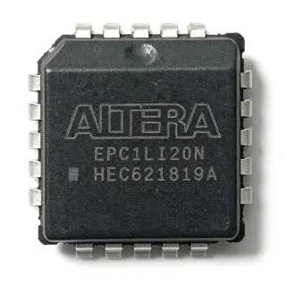
EPC2L20N - 1.6Mb Altera FPGA Config PROM | PLCC-20
MPN: EPC2L20N ✗ End of Life| Qty | Unit Price | Extended |
|---|---|---|
| 1 | $23.54 | $23.54 |
| 10 | $22.1 | $221.00 |
| 100 | $20.4 | $2,040.00 |
| 500 | $18.75 | $9,375.00 |
| 1,000 | $17.2 | $17,200.00 |
EPC2L20N Overview
What is a configuration PROM? A configuration PROM is a non-volatile serial memory that stores the FPGA's configuration bitstream and serially shifts it into the FPGA during power-up or reconfiguration. It sits between the system flash and the FPGA in the boot hierarchy: microprocessor -> flash -> configuration PROM -> SRAM-based FPGA. By isolating the bitstream from system flash, the PROM lets engineers update FPGA firmware in-system without recompiling the host firmware.
The EPC2L20N uses an in-system-programmable (ISP) interface so the bitstream can be reloaded through JTAG-style four-wire programming without removing the device from the board. Cascading of multiple PROMs is supported via the chip-enable control to handle configuration images larger than 1.6 Mb, which historically let designers support Cyclone II and APEX 20K designs. Internal oscillator and clock-management circuitry generate the serial configuration clock for the target FPGA.
The PLCC-20 (J-lead) package is through-hole-compatible and socket-compatible, allowing easy field replacement and prototype iteration. Operating temperature spans the commercial 0C to +70C range as the standard grade, with industrial-grade variants available for harsher environments.
Typical applications include Altera FPGA configuration bitstream storage for industrial control boards, telecom line cards, prototyping platforms, and embedded compute modules where the SRAM-based LUT FPGA must be reconfigured at power-up.
When designing with this device, observe Altera's configuration interface timing requirements and verify the cascaded PROM chain supports the total bitstream length for the chosen FPGA family. For new designs, designers should evaluate newer serial configuration devices, as the EPC2 family has been in mature production for many years.
This page synthesizes Altera/Intel configuration-device specifications, distributor availability and pricing, drop-in alternatives, and engineering notes not consolidated in any single manufacturer document.
Drop-in alternatives for EPC2L20N — same package, pin-to-pin compatible. Different-package parts requiring PCB rework are excluded.
Variants in this series
Same-series models that are drop-in compatible with EPC2L20N (same form factor and footprint) — differing in Mounting Type, Package, Memory Type, Supported FPGA Families, RoHS Status.
Quick Comparison Tool — Select alternative parts for side-by-side comparison:
EPC2LI20N
✅ Drop-In✓ In Stock
$5.1 / Unit
View Datasheet →EPC2LC20N
✅ Drop-In✓ In Stock
$7.4 / Unit
View Datasheet →EPC2L120N
✅ Drop-In ⚠️ 参数待验证✓ In Stock
$7.85 / Unit
View Datasheet →EPC2L20
✅ Drop-In ⚠️ 参数待验证✓ In Stock
$25.8 / Unit
View Datasheet →EPC2C20
✅ Drop-In ⚠️ 参数待验证✓ In Stock
Contact for price
View Datasheet →EPC2L20N Maximum Ratings & Electrical Characteristics
| Function | In-System Programmable Configuration PROM for SRAM-based LUT FPGAs |
| Memory Size | 1.6 Mbit |
| Programmable Type | In System Programmable (ISP) |
| Supply Voltage - VCCINT/VCCIO | 3.0 V to 3.6 V or 4.5 V to 5.5 V |
| Package / Case | 20-LCC (J-Lead), PLCC-20 |
| Packaging | Tube |
| Operating Temperature | 0C to +70C (commercial) |
| Supported FPGA Families | Altera APEX, ACEX, Cyclone, FLEX 10K, Mercury (per datasheet) |
| Configuration Interface | Serial (Altera FPP / PS configuration scheme) |
| Cascade Support | Yes (multi-PROM chain via CE control) |
| Programming Method | In-system via 4-wire ISP / JTAG-style |
| Mounting Type | Surface Mount (J-Lead PLCC) |
| Pin Count | 20 |
| Lead Finish | Matte Tin (Pb-free) |
| MSL Level | 3 (168 hours) |
| RoHS Status | Compliant |
EPC2L20N 20-lcc (j-lead), plcc-20 Pin Configuration Guide
Pin configuration for EPC2L20N (20-lcc (j-lead), plcc-20 package). This digital IC includes GPIO, communication interfaces (UART, SPI, I2C), and power pins. Refer to the manufacturer datasheet for alternate pin functions and configuration options. Essential for embedded system design and PCB layout.

No detailed pinout data available for EPC2L20N.
Refer to the datasheet for full pin configuration.
Typical Applications
EPC2L20N is suitable for 6 applications: Altera APEX 20K FPGA Configuration Storage, Altera Cyclone FPGA Bitstream Loading, Industrial Control Board Firmware Storage, Telecom Line Card FPGA Configuration, FPGA Prototyping and Development Boards, Legacy Avionics and Defense Systems.
Altera APEX 20K FPGA Configuration Storage
The EPC2L20N is purpose-built for storing the configuration bitstream of Altera APEX 20K series SRAM-based LUT FPGAs. With 1.6 Mbit of non-volatile storage per the Altera datasheet, it covers APEX 20K100 and 20K200 bitstreams when used standalone, and can be cascaded for larger 20K400/600/1000 images via the nCE chip-enable chain. The 3.0 V to 3.6 V / 4.5 V to 5.5 V dual-voltage operation lets it drive APEX configuration pins directly without external level shifters. PLCC-20 J-lead sockets simplify prototyping and field replacement.
Recommended
Altera Cyclone FPGA Bitstream Loading
Original-generation Altera Cyclone (EP1C3, EP1C6, EP1C12, EP1C20) FPGAs used the EPC2 family of configuration PROMs to load bitstream at power-up. The EPC2L20N's 1.6 Mbit matches the smaller Cyclone devices, while larger Cyclones can be served via cascaded EPC2 chains. Engineers migrating legacy Cyclone designs can drop in the EPC2L20N on existing PCBs that follow the Altera PS (passive serial) configuration scheme. ISP via four-wire programming enables field firmware updates without removing the PROM.
Recommended
Industrial Control Board Firmware Storage
Industrial control boards running legacy Altera FPGA logic (PLCs, motor controllers, machine vision front-ends) frequently use the EPC2L20N to store the FPGA firmware bitstream independent of system flash. The PLCC-20 J-lead package supports socketed mounting for easy field replacement during maintenance cycles. Operating at 3.3 V or 5 V, the EPC2L20N interfaces directly to Altera FPGAs on industrial 5 V backplanes. The in-system programmable interface lets technicians update bitstream revisions through JTAG.
Recommended
Telecom Line Card FPGA Configuration
Telecom infrastructure equipment (line cards, multiplexer shelves) built around Altera FLEX 10K and APEX 20K FPGAs relied on EPC2 PROMs for FPGA configuration. The EPC2L20N supports these designs with 1.6 Mbit storage in a socketable PLCC-20 J-lead package for serviceability. The dual-voltage (3.3 V/5 V) operation matches telecom backplane rails. Multiple PROMs can cascade via nCE to handle line-card bitstreams exceeding 1.6 Mb.
Recommended
FPGA Prototyping and Development Boards
FPGA development boards targeting Altera APEX, ACEX, Cyclone, FLEX 10K, and Mercury devices historically used the EPC2L20N for quick prototype bring-up. The PLCC-20 socketable package lets developers swap bitstreams rapidly during bring-up, and ISP allows direct in-circuit programming. The 1.6 Mbit capacity covers most early-generation Altera FPGA bitstreams. Modern development kits have transitioned to EPCQ/EPCQL SOIC-8 PROMs, but legacy boards still benefit from the EPC2L20N.
Recommended
Legacy Avionics and Defense Systems
Long-life defense and avionics platforms designed around Altera APEX 20K or FLEX 10K FPGAs continue to require EPC2 configuration PROMs through multi-decade support programs. The EPC2L20N, with its mature Altera pedigree and PLCC-20 socketable form factor, supports the obsolescence-management strategy of these programs. Industrial-temperature variants (EPC2LI20N) extend operating range for harsher environments.
Recommended
Recommended Products Summary
Engineering reference data for EPC2L20N — comparison, design guidance, and compliance information.
Selection Guide
Comparison with Alternatives
| Parameter | This Product | EPC2LI20N | EPC2LC20N | EPC2L120N | EPC2L20 | EPC2C20 |
|---|---|---|---|---|---|---|
| Brand | Altera / Intel | Altera / Intel | Altera / Intel | Altera / Intel | Altera / Intel | Altera / Intel |
| Package | PLCC-20 (J-Lead) | PLCC-20 (J-Lead) - same | PLCC-20 (J-Lead) - same | PLCC-20 (J-Lead) - same | PLCC-20 (J-Lead) - same | PLCC-20 (J-Lead) - same |
| Memory Size | 1.6 Mbit | 1.6 Mbit | 1.6 Mbit | 1.6 Mbit (variant label) | 1.6 Mbit | 1.6 Mbit (EPC2 family) |
| Supply Voltage | 3.0-3.6 V / 4.5-5.5 V | 3.0-3.6 V / 4.5-5.5 V | 3.0-3.6 V / 4.5-5.5 V | 3.0-3.6 V / 4.5-5.5 V | 3.0-3.6 V / 4.5-5.5 V | 3.0-3.6 V / 4.5-5.5 V |
| Programmable Type | In-System Programmable (ISP) | ISP | ISP | ISP | ISP | ISP |
| Function | FPGA Configuration PROM | FPGA Configuration PROM | FPGA Configuration PROM | FPGA Configuration PROM | FPGA Configuration PROM | FPGA Configuration PROM |
| Lifecycle Status | NRND | NRND | NRND | NRND | NRND | NRND |
| Operating Temperature | 0C to +70C (commercial) | Industrial grade variant | 0C to +70C (commercial) | 0C to +70C (commercial) | 0C to +70C (commercial) | 0C to +70C (commercial) |
Key Differentiators
- Mature Altera pedigree with broad legacy FPGA family support (vs EPC2LC20N)
- Documented in-system programmable (ISP) interface (vs EPC1 family (older generation))
- Dual-voltage (3.3 V / 5 V) operation in one part (vs EPCQ serial configuration devices)
Design Notes
Do not assume EPC2 family part-number suffixes (L20 vs LI20 vs LC20) are interchangeable without verifying against the manufacturer datasheet. The 'I' or 'C' suffix may denote industrial-grade temperature range or packaging variants. When designing for new production, verify the exact ordering code with Intel/Altera part-number decoder. The EPC2 family is NRNR; new designs should use EPCQ or EPCQL serial configuration devices in SOIC-8 instead.
Use a 20-pin PLCC socket for the EPC2L20N to allow field replacement during maintenance cycles and bitstream updates. Place the PROM close to the FPGA's configuration pins to minimize trace length on DCLK and DATA lines. Add 0.1 uF decoupling capacitors at VCC and VPP pins, located within 100 mils of the package. Observe the configuration interface timing diagrams in the Altera datasheet when designing cascade chains across multiple PROMs.
When cascading multiple EPC2 PROMs for bitstreams larger than 1.6 Mbit, route the nCE chip-enable signal in a daisy chain from the FPGA's nCONFIG-driven logic. Each PROM's DATA output connects to the next PROM's DATA input through a small buffer if trace length exceeds 2 inches. Refer to the Altera Configuration Devices datasheet for the exact cascade timing diagram. Maintain consistent impedance on DCLK traces to avoid configuration errors.
The EPC2L20N's configuration interface uses single-ended DCLK and DATA signals. Keep these traces short and well-separated from switching-power and high-current traces to avoid coupling noise that could cause FPGA configuration failures. Add a series damping resistor (22-33 ohm) on the DCLK output if the load is more than 4 inches or crosses multiple board layers. Verify signal integrity with the Altera configuration timing analysis tools.
Compliance Information
RoHS compliant per Altera/Intel datasheet and distributor listings. REACH, halogen-free, and conflict-mineral status not explicitly documented in the verified web data; set to 'unknown' rather than assumed. AEC-Q100 is not applicable (Altera configuration PROMs are not automotive-qualified).