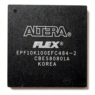
EP20K200EFC484-2X - 200K-Gate APEX-20KE FPGA, 484-FBGA | Intel
MPN: EP20K200EFC484-2X ✗ End of Life| Qty | Unit Price | Extended |
|---|---|---|
| 1 | $85 | $85.00 |
| 10 | $76.5 | $765.00 |
| 100 | $68 | $6,800.00 |
| 500 | $61.2 | $30,600.00 |
| 1,000 | $54.4 | $54,400.00 |
EP20K200EFC484-2X Overview
An FPGA is a programmable logic device (PLD) containing an array of configurable logic blocks (CLBs), embedded memory, routing interconnect, and I/O cells that engineers can program post-manufacture to implement arbitrary digital circuits. FPGAs sit in the broader semiconductor taxonomy as Application-Specific Integrated Circuit alternatives, below ASICs in NRE cost but above microcontrollers in parallel-processing throughput. The APEX-20KE family adds MultiCore interconnect and embedded ESB (Embedded System Block) memory to support system-on-a-programmable-chip (SOPC) designs.
Key features of the EP20K200EFC484-2X include 8,320 logic elements (LEs), 106,496 total RAM bits organized as embedded system blocks, 376 maximum user I/Os, and a maximum operating frequency of 205 MHz. The -2X speed grade denotes a specific performance bin within the APEX-20KE family. The 484-FBGA (23x23 mm) FineLine BGA package provides high-density interconnect while remaining compatible with surface-mount PCB assembly lines.
The device architecture combines four-input look-up tables (LUTs) per LE with MultiCore routing, embedded CAM, dual-port RAM, and content-addressable memory support. The 1.8 V core voltage reduces dynamic power compared to 2.5 V predecessors, and the I/O banks support multiple I/O standards including LVTTL, LVCMOS, and PCI.
Typical applications include telecom line cards, industrial control logic, glue logic replacement, high-speed DSP pre-processing, and ASIC prototyping. The 200K-gate density is well matched to mid-complexity bus-bridging designs, video processing, and parallel interface aggregation.
When designing with this part, ensure proper decoupling of all VCCINT and VCCIO rails and follow Altera AN 116 guidelines for APEX 20KE power-up sequencing. The 484-BGA package requires careful PCB layout with microvia technology for signal escape.
This page synthesizes distributor pricing, drop-in pin-compatible alternatives, and practical design notes that supplement the manufacturer datasheet and reference designs.
Drop-in alternatives for EP20K200EFC484-2X — same package, pin-to-pin compatible. Different-package parts requiring PCB rework are excluded.
Variants in this series
Same-series models that are drop-in compatible with EP20K200EFC484-2X (same form factor and footprint) — differing in Package, Operating Temperature, Speed Grade, Family, Propagation Delay.
Quick Comparison Tool — Select alternative parts for side-by-side comparison:
EP20K200EFC484-1X
✅ Drop-In✓ In Stock
$165 / Unit
View Datasheet →EP20K200EFC484-2N
✅ Drop-In✓ In Stock
$175 / Unit
View Datasheet →EP20K200EFC484-1N
✅ Drop-In✓ In Stock
$290 / Unit
View Datasheet →EP20K200EFC484-1
✅ Drop-In✓ In Stock
$68.4 / Unit
View Datasheet →EP20K200BC484-1X
✅ Drop-In✓ In Stock
$75.1 / Unit
View Datasheet →EP20K200EFC484-2X Maximum Ratings & Electrical Characteristics
| Family | APEX-20KE |
| Logic Elements | 8,320 |
| LABs/CLBs | 832 |
| Total RAM Bits | 106,496 |
| Gate Count | 200,000 |
| User I/O Pins | 376 |
| Max Operating Frequency | 205 MHz |
| Core Supply Voltage (VCCINT) | 1.71 V to 1.89 V (1.8 V nominal) |
| I/O Supply Voltage (VCCIO) | 3.3 V / 2.5 V (multi-standard) |
| Process Technology | 0.22 µm CMOS |
| Package | 484-FBGA (23x23 mm) |
| Package Code | BGA, Ball, Square |
| Propagation Delay | 2.5 ns |
| Operating Temperature | 0 °C to 85 °C |
| Speed Grade | -2X |
EP20K200EFC484-2X bga, ball, square Pin Configuration Guide
Pin configuration for EP20K200EFC484-2X (bga, ball, square package). This digital IC includes GPIO, communication interfaces (UART, SPI, I2C), and power pins. Refer to the manufacturer datasheet for alternate pin functions and configuration options. Essential for embedded system design and PCB layout.

No detailed pinout data available for EP20K200EFC484-2X.
Refer to the datasheet for full pin configuration.
Typical Applications
EP20K200EFC484-2X is suitable for 6 applications: Telecom Line Card Glue Logic, Industrial Motor Control, ASIC Prototyping, Video Processing & Image Aggregation, High-Speed Data Acquisition, Military & Aerospace Legacy Systems.
Telecom Line Card Glue Logic
The EP20K200EFC484-2X's 8,320 logic elements and 376 user I/Os are well matched to telecom line-card glue-logic functions, including Utopia/UTOPIA-3 bus multiplexing, DS3/E3 framers, and TDM switch fabric interfacing. The 1.8 V core reduces power dissipation across densely populated line cards while the 205 MHz Fmax supports 155 Mbps POS-PHY or higher backplane interconnect. According to the manufacturer datasheet, the MultiCore architecture allows multiple glue-logic functions to be partitioned into separate logic blocks for cleaner timing closure. The 106,496 bits of embedded RAM enable on-chip buffering of cell/packet descriptors, eliminating external SRAM on per-channel basis. Compared to a discrete ASIC implementation, the EP20K200EFC484-2X cuts NRE cost to zero while delivering similar per-channel logic density in a 484-FBGA package.
Recommended
Industrial Motor Control
The EP20K200EFC484-2X integrates DSP pre-processing, PWM generation, and encoder feedback logic in industrial motor-control drives up to 200K gates of logic complexity. Its 376 user I/Os are sufficient for multi-axis servo control (up to 3 axes) with parallel QEP/Hall sensor input, 3-phase PWM outputs, and EtherCAT/CANopen external MAC interfaces. The 1.71 V to 1.89 V core supply simplifies integration with 3.3 V digital isolators, and the 0 °C to 85 °C operating range covers factory-floor cabinet environments. According to the manufacturer datasheet, the embedded system block (ESB) memory provides dual-port RAM for ping-pong PWM sample buffers, eliminating wait states. Designers should pair the FPGA with a high-speed ADC (e.g., 16-bit SAR) for current/voltage sensing and leverage the FPGA's parallel arithmetic paths for Park/Clarke transforms in real time.
Recommended
ASIC Prototyping
The EP20K200EFC484-2X is widely used for ASIC prototyping and pre-silicon verification, where the 200K-gate density closely matches mid-complexity ASIC designs and the 484-FBGA package provides generous pin count for verification headers. The MultiCore architecture with 832 LABs/CLBs enables partitioning of the prototype logic along the same boundaries as the target ASIC, simplifying timing correlation. The 106,496 bits of embedded RAM model internal ASIC SRAM blocks with reasonable accuracy. According to the manufacturer datasheet, JTAG-based configuration allows unlimited reprogram cycles during verification. The 1.8 V core is compatible with most modern ASIC process nodes, simplifying I/O model translation. For teams migrating prototypes to ASIC, the Quartus II tool chain provides timing and synthesis reports in industry-standard formats (SDC, SDF).
Recommended
Video Processing & Image Aggregation
The EP20K200EFC484-2X suits parallel video processing applications such as multi-camera aggregation, video format conversion, and frame-rate conversion up to HD (1080p60) resolution. The 376 user I/Os accommodate parallel BT.1120/ITU-R BT.656 video buses from multiple camera inputs plus a high-speed memory bus (DDR/QDR SRAM interface) for frame buffering. The 8,320 logic elements and 106,496 RAM bits enable 2D filter cores, color-space converters, and scaling pipelines. According to the manufacturer datasheet, the LVDS-capable I/O supports Cameralink and Channel Link physical layers for industrial vision systems. The 205 MHz system frequency is adequate for parallel-pixel processing at HD rates. For multi-channel capture, multiple EP20K200EFC484-2X devices can be ganged with shared clocking.
Recommended
High-Speed Data Acquisition
The EP20K200EFC484-2X enables high-speed data acquisition systems with on-chip preprocessing of ADC samples at rates up to 205 MHz. Typical use cases include digital oscilloscope front-ends, software-defined radio (SDR) baseband preprocessing, and radar return pre-processing. The 8,320 logic elements implement FIR filters, FFT butterflies, and digital down-conversion (DDC) chains for IF-to-baseband conversion. The 106,496-bit embedded memory acts as a sample buffer between ADC bursts and the host processor. According to the manufacturer datasheet, the LVDS I/O supports direct interfacing with parallel-output ADCs (e.g., 12-/14-bit ADCs at 100-200 MSPS) without external buffers. The 1.8 V core reduces switching noise that would otherwise couple into analog front-ends.
Recommended
Military & Aerospace Legacy Systems
Although the EP20K200EFC484-2X itself is not military-grade qualified (0 °C to 85 °C commercial), it is widely used in legacy military and aerospace subsystem designs originally built around the APEX-20KE family. Designers maintaining or refurbishing fielded systems need pin-compatible replacements to sustain MRO operations. The 484-FBGA footprint and 8,320 logic elements match the original design's interface contract exactly, eliminating PCB rework. According to the manufacturer datasheet, the device supports JTAG boundary-scan for in-system verification during depot-level maintenance. For new defense programs, designers should evaluate Cyclone IV or Stratix V/V10 equivalents with proper MIL-PRF-38535 screening rather than this obsolete commercial-grade part.
Recommended
Recommended Products Summary
Engineering reference data for EP20K200EFC484-2X — comparison, design guidance, and compliance information.
Selection Guide
Comparison with Alternatives
| Parameter | This Product | EP20K200EFC484-1X | EP20K200EFC484-2N | EP20K200EFC484-1N | EP20K200EFC484-1 | EP20K200BC484-1X |
|---|---|---|---|---|---|---|
| Brand | Intel (formerly Altera) | Intel (formerly Altera) | Intel (formerly Altera) | Intel (formerly Altera) | Intel (formerly Altera) | Intel (formerly Altera) |
| Package | 484-FBGA (23x23 mm) | 484-FBGA (23x23 mm) - same | 484-FBGA (23x23 mm) - same | 484-FBGA (23x23 mm) - same | 484-FBGA (23x23 mm) - same | 484-FBGA - same |
| Family | APEX-20KE | APEX-20KE | APEX-20KE | APEX-20KE | APEX-20KE | APEX-20KE |
| Logic Elements | 8,320 | 8,320 | 8,320 | 8,320 | 8,320 | 8,320 |
| Total RAM Bits | 106,496 | 106,496 | 106,496 | 106,496 | 106,496 | 106,496 |
| User I/Os | 376 | 376 | 376 | 376 | 376 | 376 |
| Core Voltage | 1.71 V to 1.89 V (1.8 V nominal) | 1.71 V to 1.89 V | 1.71 V to 1.89 V | 1.71 V to 1.89 V | 1.71 V to 1.89 V | 1.71 V to 1.89 V |
| Lifecycle Status | Obsolete | Obsolete | Obsolete | Obsolete | Obsolete | Obsolete |
Key Differentiators
- Higher maximum operating frequency (vs EP20K200EFC484-1X)
- Same 484-FBGA footprint enables drop-in upgrade path (vs EP20K200BC484-1X)
- Pinned to APEX-20KE architecture for legacy design continuity (vs Cyclone IV EP4CE6 (modern alternative))
Design Notes
The EP20K200EFC484-2X requires a stable 1.71 V to 1.89 V (1.8 V nominal) core supply on VCCINT pins and separate VCCIO rails for each I/O bank. Per Altera AN 116, place 0.1 µF ceramic decoupling capacitors within 5 mm of every VCCINT ball and bulk 33 µF tantalum capacitors on each VCCIO bank. Power-up sequencing should ramp VCCINT first, then VCCIO, with the JTAG configuration pins held in reset until supplies stabilize. Estimated: with 200K gates active at 50% toggle rate, dynamic current may reach ~500 mA - refer to APEX-20KE power calculator for exact figure.
The 484-FBGA (23x23 mm) FineLine BGA package requires microvia PCB technology for clean signal escape. Use a 1.0 mm or 1.27 mm ball pitch with fanout to 4 inner signal layers. The thermal pad (if present) must be soldered to a copper pour with thermal vias. Per APEX-20KE hardware reference manual, the 23x23 mm package dissipates up to 3 W at full activity without airflow, requiring at least 10 thermal vias to an inner copper plane.
The APEX-20KE family uses 1.8 V I/O standards which are incompatible with 3.3 V LVTTL inputs without level shifting. Common mistakes include: (1) connecting LVCMOS33 signals directly to APEX-20KE VCCIO=1.8V banks, which overdrives the inputs; (2) attempting to program the device with the wrong Quartus II version - use Quartus II v9.1 or earlier with appropriate APEX-20KE support; (3) ignoring CONFIG_DONE pin polarity in JTAG chain design; (4) substituting a 5 V-tolerant I/O bank where one is not present.
For high-speed interfaces above 100 MHz (LVDS, DDR), follow Altera AN 224 (High-Speed Board Design for APEX 20KE) guidelines: matched differential pair length within 25 mil tolerance, ground reference plane continuity, and 45-ohm single-ended / 90-ohm differential impedance. The 484-FBGA fanout should prioritize high-speed signals on top layer escape to avoid via stubs. Clock inputs should be routed with 50-ohm controlled impedance and isolated from switching I/O by ground guard traces.
Compliance Information
Compliance status not confirmed in the verified web data; the part is obsolete and was originally released before strict RoHS/REACH enforcement. Designers should request a Certificate of Compliance from authorized distributors for production use.