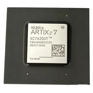
EP4CE40F23C9LN - 39,600-Cell FPGA | Intel | Embedded Logic
MPN: EP4CE40F23C9LN ✓ Active| Qty | Unit Price | Extended |
|---|---|---|
| 1 | $92 | $92.00 |
| 10 | $88 | $880.00 |
| 100 | $82 | $8,200.00 |
| 500 | $76 | $38,000.00 |
| 1,000 | $69 | $69,000.00 |
EP4CE40F23C9LN Overview
A field-programmable gate array, or FPGA, is a semiconductor device built from programmable logic elements, routing resources, input/output blocks, and embedded functional blocks. Its configuration can be changed after circuit-board assembly. Within the system hierarchy, the FPGA sits between fixed-function processors and custom integrated circuits: it offers more deterministic parallel processing than a general-purpose processor while avoiding the high nonrecurring engineering cost of an application-specific integrated circuit.
The principal capacity figures are 39,600 logic cells and 2,475 CLBs, supported by 328 I/Os in the 484-ball package. The supplied data also reports 1,161,216 bits, a 23 mm by 23 mm body, and 1 mm pitch. These attributes make the device suitable for bridges, state-machine implementations, instrument control, industrial automation, and moderate-density digital processing. Configuration storage, embedded blocks, and supported I/O standards must be confirmed in the complete manufacturer datasheet before release to production.
Cyclone IV E devices are offered with 1.0 V or 1.2 V core-voltage variants, according to the manufacturer-family material provided. The C9 ordering designation and the F23 package code identify the commercial-speed, 484-ball implementation. The distinction between the 265 MHz listed frequency and 472 MHz internal-frequency entry should be resolved against the applicable timing tables and operating conditions rather than treated as one interchangeable performance rating.
Typical uses include industrial controllers, communications-interface aggregation, test equipment, image preprocessing, motor-control sequencing, and educational or prototyping platforms. The 328 available I/Os are useful when many parallel sensors, converters, memories, or control peripherals must be connected. Firmware-like FPGA configuration data, power sequencing, decoupling, clock integrity, and pin-compatible substitution must be evaluated as part of system validation.
Designers should preserve the exact 484-ball FBGA land pattern, validate all bank-specific I/O voltages, and confirm timing with the intended speed grade and configuration mode. A search result describing EP4CE6E22C8 does not establish package or pin compatibility; it should not be used as a drop-in substitute without complete pinout and parametric verification.
This page combines the verified distributor specifications, official ordering-part information, same-family ordering options, explicit data-needed markers, and a drop-in analysis that requires package, pinout, and parameter evidence. It is intended to reduce sourcing ambiguity while keeping unverified electrical, thermal, lifecycle, compliance, and supply claims separate from confirmed values.
Drop-in alternatives for EP4CE40F23C9LN — same package, pin-to-pin compatible. Different-package parts requiring PCB rework are excluded.
Variants in this series
Same-series models that are drop-in compatible with EP4CE40F23C9LN (same form factor and footprint) — differing in Package, Speed Grade, Process Technology, Operating Temperature, RoHS Status.
Quick Comparison Tool — Select alternative parts for side-by-side comparison:
EP4CE40F23C9L
✅ Drop-In✓ In Stock
$48.8 / Unit
View Datasheet →EP4CE40F23C8N7N
✅ Drop-In✓ In Stock
$112.85 / Unit
View Datasheet →EP4CE40F23C8N
✅ Drop-In✓ In Stock
$52.95 / Unit
View Datasheet →EP4CE40F23C8LN
✅ Drop-In✓ In Stock
$49.95 / Unit
View Datasheet →EP4CE40F23C8L
✅ Drop-In✓ In Stock
$72.1 / Unit
View Datasheet →EP4CE40F23C9LN Maximum Ratings & Electrical Characteristics
| Device Type | Field Programmable Gate Array |
| FPGA Family | Cyclone IV E |
| Logic Cells | 39,600 |
| Configurable Logic Blocks | 2,475 |
| Embedded Memory | 1,161,216 bit |
| User I/O Count | 328 |
| Listed Frequency | 265 MHz |
| Internal Frequency | 472 MHz |
| Package | FBGA-484 |
| Package Dimensions | 23 mm x 23 mm |
| Ball Pitch | 1 mm |
| Ball Count | 484 |
| Terminal Form | Ball |
| Core Voltage Option 1 | 1.0 V |
| Core Voltage Option 2 | 1.2 V |
| Lead-Free Status | Lead free |
EP4CE40F23C9LN 23 mm x 23 mm Pin Configuration Guide
Pin configuration for EP4CE40F23C9LN (23 mm x 23 mm package). This digital IC includes GPIO, communication interfaces (UART, SPI, I2C), and power pins. Refer to the manufacturer datasheet for alternate pin functions and configuration options. Essential for embedded system design and PCB layout.

No detailed pinout data available for EP4CE40F23C9LN.
Refer to the datasheet for full pin configuration.
Typical Applications
EP4CE40F23C9LN is suitable for 6 applications: Industrial Automation Controller, Communications Interface Bridge, Test and Measurement Instrument, Motor-Control Sequencing, Image and Sensor Data Preprocessing, Digital System Prototyping.
Industrial Automation Controller
EP4CE40F23C9LN fits an industrial automation controller when the design needs deterministic parallel logic and a high number of external connections. Its verified 39,600 logic cells, 2,475 configurable logic blocks, 1,161,216 embedded-memory bits, and 328 user I/Os provide resources for sensor aggregation, protocol conversion, safety-state sequencing, and timing control. The device can implement multiple independent logic paths while retaining programmable behavior. Engineers should confirm the required commercial temperature range, I/O-bank voltages, clocking resources, and environmental compliance before deployment. The 484-ball FBGA package also requires controlled assembly and a verified PCB land pattern; it is not a through-hole replacement.
Recommended
Communications Interface Bridge
EP4CE40F23C9LN can serve as a communications-interface bridge between parallel buses, serial transceivers, memory controllers, and application processors. The 328 I/Os are useful for adapting data widths, buffering packets, managing handshakes, and performing clock-domain isolation in hardware. Its 39,600 logic cells and 1,161,216 embedded-memory bits allow moderate buffering and packet-processing functions without consuming all resources on a larger FPGA. Exact I/O standards, bank limits, supported clock frequencies, and transceiver requirements are not established by the supplied snippets. Validate those parameters in the official family documentation and confirm whether the application needs only general-purpose I/O or a device with dedicated high-speed interfaces.
Recommended
Test and Measurement Instrument
EP4CE40F23C9LN is a plausible programmable logic platform for test and measurement equipment that requires parallel acquisition, timing generation, stimulus sequencing, and data formatting. The verified 2,475 configurable logic blocks and 39,600 logic cells can implement counters, state machines, trigger logic, and multiple acquisition channels. Its 328 I/Os help connect converters, sensors, control signals, and display or communication peripherals. The 265 MHz listed frequency and 472 MHz internal-frequency entry should not be used interchangeably; the actual clock and timing budget must be taken from the applicable device documentation. A production design should also analyze thermal behavior, power integrity, configuration reliability, and the 23 mm by 23 mm 484-ball PCB implementation.
Recommended
Motor-Control Sequencing
EP4CE40F23C9LN can be used for motor-control sequencing, encoder acquisition, commutation logic, protection handling, and communication with a supervisory controller. The device’s 39,600 logic cells and 2,475 configurable logic blocks provide space for deterministic control loops and parallel I/O management, while 328 user I/Os support encoder, gate-driver, analog-front-end, and network interfaces. The supplied data does not confirm industrial temperature qualification, automotive qualification, or dedicated motor-control peripherals, so the design must not assume them. Verify every I/O-bank voltage, timing constraint, clock input, and protection response. The 484-ball FBGA package is suitable for compact boards but requires thermal and assembly review for continuous industrial operation.
Recommended
Image and Sensor Data Preprocessing
EP4CE40F23C9LN can preprocess parallel image or sensor data before forwarding it to a processor, memory, or display subsystem. The verified 1,161,216 embedded-memory bits and 39,600 logic cells can support line buffers, filtering, thresholding, packetization, and timing synchronization. Its 328 I/Os are useful when multiple cameras, sensors, or converters must be connected simultaneously. Actual pixel throughput cannot be inferred from the listed 265 MHz or 472 MHz values; it depends on internal architecture, memory usage, I/O standards, clocking, and routing constraints. Engineers should estimate resource utilization in the selected toolchain, simulate the complete datapath, and verify that the selected configuration fits without consuming routing or power margin.
Recommended
Digital System Prototyping
EP4CE40F23C9LN is useful for digital-system prototypes that need more capacity than a small CPLD while retaining a programmable development path. The 39,600 logic cells, 2,475 configurable logic blocks, and 1,161,216 embedded-memory bits allow engineers to test bus controllers, data paths, state machines, and custom peripherals before committing to fixed logic. Its 328 I/Os provide access to many external signals, and the 484-ball FBGA package encourages a structured, high-density board layout. The design must use the correct configuration method, clocking resources, power rails, and I/O-bank assignments. Because the supplied material does not provide a full pinout or thermal limits, obtain the manufacturer package and device documentation before schematic release.
Recommended
Recommended Products Summary
Engineering reference data for EP4CE40F23C9LN — comparison, design guidance, and compliance information.
Selection Guide
Comparison with Alternatives
| Parameter | This Product | EP4CE40F23C9L | EP4CE40F23C8N7N | EP4CE40F23C8N | EP4CE40F23C8LN | EP4CE40F23C8L |
|---|---|---|---|---|---|---|
| Brand | Intel | Intel | Intel | Intel | Intel | Intel |
| Package | FBGA-484 | FBGA-484 | FBGA-484 | FBGA-484 | FBGA-484 | FBGA-484 |
Key Differentiators
- Higher verified logic capacity than a smaller Cyclone device result (vs EP4CE6E22C8)
- High verified user-I/O count (vs EP4CE6E22C8)
- Large embedded-memory resource (vs EP4CE6E22C8)
- Same-family sourcing breadth (vs EP4CE40F23C8N7N)
Design Notes
Start the power design from the manufacturer’s exact device-family documentation rather than assuming that every Cyclone IV E variant uses the same rail set. The verified material says the family is offered with 1.0 V or 1.2 V core-voltage variants, but it does not provide the complete EP4CE40F23C9LN power table. Confirm core, analog, configuration, and I/O-bank requirements for the exact ordering code. Place local decoupling close to the relevant power balls, provide a defined power-up sequence, and keep high-current switching paths away from clock and configuration inputs. Validate rail tolerances and transient behavior on the assembled board.
Use the official 23 mm by 23 mm, 1 mm-pitch, 484-ball FBGA package drawing as the only source for land geometry, ball numbering, and escape recommendations. The supplied search results confirm the package family but do not include the complete pin table. Preserve the same footprint and pin numbering for any candidate, and use a controlled-impedance stack-up for high-speed clocks and differential or memory interfaces. Verify solder-paste, via-in-pad, and BGA-assembly processes with the board fabricator. Inspect the assembled package for bridging and open joints, especially when the design uses many simultaneous switching I/Os.
Treat the 265 MHz listed frequency and 472 MHz internal-frequency entry as different values requiring definition from the applicable datasheet and timing tools. Do not calculate data throughput directly from either value without accounting for logic depth, routing delay, clock uncertainty, I/O standards, and embedded-memory behavior. Constrain every clock and high-speed interface, preserve the manufacturer-recommended termination and reference-voltage connections, and simulate the complete design at the intended voltage and temperature. Check the generated configuration for excessive fanout, routing congestion, and simultaneous-switching noise before programming hardware.
Thermal data for EP4CE40F23C9LN is not supplied in the verified snippets, so junction temperature, allowable power dissipation, and package thermal resistance are [DATA_NEEDED: thermal limits]. Use the manufacturer device documentation and an application-specific power estimate before selecting a cooling strategy. Measure the board in its final enclosure, airflow, altitude, and operating voltage conditions. Spread heat through the permitted PCB copper and vias, keep thermal paths away from sensitive analog references, and use temperature sensors or margin checks during validation. Do not present a calculated junction temperature as a guaranteed datasheet limit.
Do not select an FPGA using only the family name, the 39,600-cell headline, or a distributor’s generic frequency entry. Confirm the exact ordering code, package drawing, pinout, I/O-bank limits, configuration method, supported memory interfaces, and timing grade. Same-family candidates such as EP4CE40F23C8N7N and EP4CE40F23C8N must not be treated as drop-ins without comparison of every suffix field. A 484-ball BGA cannot be interchanged with a smaller package, and a search result that compares a different device does not prove pin compatibility. Build a controlled BOM, qualify alternates, and re-run schematic, PCB, simulation, and power checks.
Compliance Information
The verified search snippets identify the part as lead free, but do not provide RoHS, REACH, halogen-free, AEC-Q100, or conflict-minerals declarations. AEC-Q100 is not applicable to the supplied evidence; no automotive qualification is claimed.