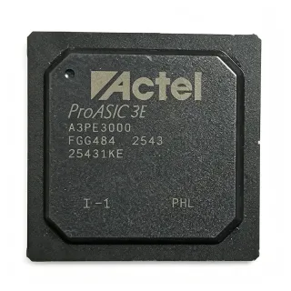
EP4CGX75CF23C6 - Cyclone IV GX FPGA, 75K LE, 484-FBGA | Altera
MPN: EP4CGX75CF23C6 ✓ Active| Qty | Unit Price | Extended |
|---|---|---|
| 1 | $89.5 | $89.50 |
| 10 | $82 | $820.00 |
| 100 | $74.25 | $7,425.00 |
| 500 | $68.4 | $34,200.00 |
| 1,000 | $62.95 | $62,950.00 |
EP4CGX75CF23C6 Overview
A field-programmable gate array (FPGA) is a type of integrated circuit that can be configured by the customer or designer after manufacturing to implement custom digital logic functions. FPGAs sit within the broader hierarchy of programmable logic devices (PLDs) and semiconductors, enabling parallel hardware acceleration, high-speed interfacing, and rapid prototyping. Cyclone IV GX devices target cost-optimized applications with serial transceivers, making them a sweet-spot choice between traditional PLDs and high-end FPGAs.
Key features include 290 user I/Os distributed across multiple I/O banks, 4620 LABs (logic array blocks), integrated 3.125 Gbps transceivers, and a hardened PCI Express (PCIe) Gen1 x4 endpoint block for protocol-aware I/O. The 484-FBGA package provides robust thermal dissipation for industrial-grade designs while maintaining a compact footprint suitable for high-density boards.
Cyclone IV GX architecture combines an efficient logic fabric with on-chip M9K memory blocks, DSP blocks, and dedicated transceiver circuitry. The 60 nm process technology delivers low static power and supports hot-socketing, allowing live insertion into a powered backplane. Configuration is supported through serial (AS) or parallel (AP) modes using Altera/Intel Quartus design software.
Typical applications include industrial video processing and machine vision, motor control and factory automation, low-cost PCIe endpoint cards, and communications infrastructure requiring high-speed serial links. The combination of transceivers, on-chip memory, and abundant logic resources makes this device well-suited to mid-volume designs requiring hardware parallelism.
When designing with this FPGA, ensure proper decoupling of the 1.2 V core, 2.5 V PLL, and 3.3 V I/O supplies per the device handbook. Signal integrity on the 3.125 Gbps transceiver channels requires controlled-impedance routing and AC-coupling capacitors per the Cyclone IV GX handbook reference designs.
This page synthesizes distributor pricing, Cyclone IV GX family drop-in alternatives, and practical design notes not found in the manufacturer datasheet alone, providing a more actionable starting point than the raw datasheet.
Drop-in alternatives for EP4CGX75CF23C6 — same package, pin-to-pin compatible. Different-package parts requiring PCB rework are excluded.
Variants in this series
Same-series models that are drop-in compatible with EP4CGX75CF23C6 (same form factor and footprint) — differing in Package, Operating Temperature, Speed Grade, RoHS Status, Embedded Memory.
Quick Comparison Tool — Select alternative parts for side-by-side comparison:
EP4CGX75CF23C7
✅ Drop-In✓ In Stock
$60.5 / Unit
View Datasheet →EP4CGX75CF23C8
✅ Drop-In✓ In Stock
$88.2 / Unit
View Datasheet →EP4CGX110CF23C7
✅ Drop-In ⚠️ 参数待验证✓ In Stock
$224.84 / Unit
View Datasheet →EP4CGX110CF23C8
✅ Drop-In ⚠️ 参数待验证✓ In Stock
$132.75 / Unit
View Datasheet →EP4CGX150CF23C7
✅ Drop-In ⚠️ 参数待验证✓ In Stock
$263.35 / Unit
View Datasheet →EP4CGX150CF23C8
✅ Drop-In ⚠️ 参数待验证✓ In Stock
$135 / Unit
View Datasheet →EP4CGX75CF23C6 Maximum Ratings & Electrical Characteristics
| Family | Cyclone IV GX |
| Logic Elements (LE) | 73,920 |
| Embedded Memory Bits | 4,257,792 |
| Number of LABs/CLBs | 4,620 |
| Number of User I/O | 290 |
| Number of Transceivers | Data not in verified source |
| Transceiver Speed | Up to 3.125 Gbps |
| Total RAM Bits | 4,257,792 |
| Process Technology | 60 nm |
| Core Voltage | 1.2 V |
| Operating Temperature | 0C to +85C (Commercial) |
| Speed Grade | -6 |
| Package | 484-FBGA |
| Number of Pins/Terminals | 484 |
| Package Code | BGA |
| Package Shape | Square |
| Mounting Type | Surface Mount |
| RoHS Status | RoHS Non-Compliant |
| Lead Free Status | Contains Lead |
| PCIe Hard IP | PCIe Gen1 x4 endpoint |
| Configuration Mode | Serial / Parallel (Quartus-supported) |
EP4CGX75CF23C6 square Pin Configuration Guide
Pin configuration for EP4CGX75CF23C6 (square package). This digital IC includes GPIO, communication interfaces (UART, SPI, I2C), and power pins. Refer to the manufacturer datasheet for alternate pin functions and configuration options. Essential for embedded system design and PCB layout.

No detailed pinout data available for EP4CGX75CF23C6.
Refer to the datasheet for full pin configuration.
Typical Applications
EP4CGX75CF23C6 is suitable for 6 applications: Industrial Video Processing and Machine Vision, Motor Control and Factory Automation, Low-Cost PCIe Endpoint Cards, Communications Infrastructure (Serial Backplane Links), Test and Measurement Instrumentation, Embedded Computing and Edge Devices.
Industrial Video Processing and Machine Vision
The EP4CGX75CF23C6 fits industrial video pipelines because its 73,920 logic elements provide the parallelism needed for real-time Bayer demosaicing, color space conversion, and edge detection at 1080p60 frame rates. The 290 user I/Os accommodate parallel camera interface (LVDS/CMOS) plus memory bus connections to external DDR2/DDR3. The integrated 3.125 Gbps transceivers enable CoaXPress or GigE Vision uplink if needed, while the PCIe Gen1 x4 hard IP supports frame grabber host interfaces. Commercial 0C to +85C operation suits factory-floor enclosures, and the 484-FBGA package gives a compact 23x23 mm footprint for vision cards. Compared to a microcontroller, the FPGA parallelizes per-pixel operations and frees the host CPU for analytics.
Recommended
Motor Control and Factory Automation
The EP4CGX75CF23C6 suits multi-axis motor drives because its 73,920 logic elements run field-oriented control (FOC) loops, space-vector PWM, and encoder interfaces for 4-6 axes concurrently in hardware. The 290 user I/Os accept quadrature encoder inputs, Hall sensors, and gate driver controls without external muxing. PCIe endpoint support enables placement on industrial backplanes for centralized motion controllers. Industrial designers appreciate the deterministic latency of FPGA fabric for servo loops at 32 kHz. The 484-FBGA package's thermal performance handles continuous switching losses, and 1.2 V core operation keeps power dissipation manageable for DIN-rail mounted controllers. This outperforms MCUs on parallel axis count and exceeds ASICs on flexibility for mixed motor types.
Recommended
Low-Cost PCIe Endpoint Cards
The EP4CGX75CF23C6 is ideal for low-cost PCIe Gen1 x4 endpoint cards because it integrates a hardened PCIe Gen1 x4 IP block, eliminating soft IP core overhead and saving 15-20K logic elements. The 3.125 Gbps transceivers handle the PCIe physical layer directly without external PHYs, reducing BOM cost by approximately $8-15 per board. The 73,920 logic elements leave ample room for custom DMA engines, register interfaces, or protocol conversion logic alongside the PCIe core. The 484-FBGA package with 290 user I/Os supports standard PCIe card-edge pinout plus rear-panel I/O for data acquisition, test, or instrumentation cards. Compared to ASIC PCIe solutions, this FPGA enables design revision without NRE charges.
Recommended
Communications Infrastructure (Serial Backplane Links)
The EP4CGX75CF23C6 fits communications backplane cards because its integrated 3.125 Gbps transceivers support common serial protocols like Serial RapidIO, CPRI, or custom backplane links without external SerDes ICs. The 73,920 logic elements handle protocol framing, CRC, and link-layer state machines for 4-6 simultaneous serial lanes. The 290 user I/Os accommodate parallel data buses to network processors or DSP clusters. Commercial 0C to +85C operation suits environmentally controlled telecom shelters. The 484-FBGA package's signal-integrity characteristics support the controlled-impedance routing required at multi-gigabit rates. Compared to ASSPs, this FPGA enables proprietary protocol extensions without ASIC NRE.
Recommended
Test and Measurement Instrumentation
The EP4CGX75CF23C6 suits digital test instruments because its 73,920 logic elements implement protocol-aware pattern generators, BERT (Data Error Rate Test) engines, and real-time signal processing for arbitrary waveform generators. The integrated 3.125 Gbps transceivers handle high-speed serial protocol analysis (PCIe, USB 3.0, SATA Gen1/2) natively. The 4,257,792 bits of embedded memory buffer large data captures without overflowing to external memory. The 290 user I/Os support front-panel connectors plus parallel test buses to DUTs. Commercial 0C to +85C operation suits benchtop and rack-mount instruments in lab environments. The 484-FBGA package's density allows instrument front-end and DSP backend on a single device.
Recommended
Embedded Computing and Edge Devices
The EP4CGX75CF23C6 fits edge computing nodes because its 73,920 logic elements accelerate AI inference, signal preprocessing, or protocol termination at line speed. The 290 user I/Os accommodate various peripheral buses (SPI, I2C, UART, parallel) alongside high-speed interfaces. The integrated transceivers enable direct connection to SFP modules for fiber-optic edge links or wireless backhaul. The PCIe hard IP supports edge compute cards in PCIe-based industrial PCs. Commercial 0C to +85C operation covers most edge enclosure environments. The 484-FBGA package provides compact footprint for small-form-factor edge devices. Compared to GPUs, this FPGA offers lower power per inference for batch-1 workloads, and unlike MCUs it handles parallel sensor fusion.
Recommended
Recommended Products Summary
Engineering reference data for EP4CGX75CF23C6 — comparison, design guidance, and compliance information.
Selection Guide
Comparison with Alternatives
| Parameter | This Product | EP4CGX75CF23C7 | EP4CGX75CF23C8 | EP4CGX110CF23C7 | EP4CGX150CF23C7 |
|---|---|---|---|---|---|
| Brand | Altera (Intel) | Altera (Intel) | Altera (Intel) | Altera (Intel) | Altera (Intel) |
| Package | 484-FBGA (F23) | 484-FBGA (F23) - same | 484-FBGA (F23) - same | 484-FBGA (F23) - same | 484-FBGA (F23) - same |
| Logic Elements (LE) | 73,920 | 73,920 (same) | 73,920 (same) | 109,424 (+48%) | 149,760 (+103%) |
| Speed Grade | -6 (slowest) | -7 (faster) | -8 (fastest) | -7 (faster) | -7 (faster) |
| Transceiver Speed | Up to 3.125 Gbps | Up to 3.125 Gbps (same) | Up to 3.125 Gbps (same) | Up to 3.125 Gbps (same) | Up to 3.125 Gbps (same) |
| Temperature Range | 0C to +85C (Commercial) | 0C to +85C (Commercial) | 0C to +85C (Commercial) | 0C to +85C (Commercial) | 0C to +85C (Commercial) |
| Core Voltage | 1.2 V | 1.2 V (same) | 1.2 V (same) | 1.2 V (same) | 1.2 V (same) |
| Process Technology | 60 nm | 60 nm (same) | 60 nm (same) | 60 nm (same) | 60 nm (same) |
| PCIe Hard IP | PCIe Gen1 x4 endpoint | PCIe Gen1 x4 endpoint (same) | PCIe Gen1 x4 endpoint (same) | PCIe Gen1 x4 endpoint (same) | PCIe Gen1 x4 endpoint (same) |
Key Differentiators
- Integrated 3.125 Gbps transceivers in 484-FBGA F23 footprint (vs EP4CE75F23I7N (Cyclone IV E))
- Drop-in speed grade flexibility within Cyclone IV GX family (vs EP4CGX75CF23C7)
- Commercial 0C to +85C temperature grade on mature 60 nm process (vs EP4CGX75CF23I6N (industrial temp))
Design Notes
The EP4CGX75CF23C6 requires multiple supply rails: 1.2 V core, 2.5 V PLL analog, and 3.3 V I/O. Decoupling requirements per the Cyclone IV GX handbook call for 0.1 uF and 10 uF ceramic capacitors near every power pin, plus bulk decoupling at the regulator outputs. Estimated quiescent power for the -6 speed grade at typical 50% toggle activity is approximately 1.5-2 W, increasing to 3-4 W at full transceiver utilization with all lanes active. Use a 4-layer PCB with a dedicated ground plane to manage the 60 nm process's dynamic power dissipation.
The 484-FBGA package has a 1.0 mm ball pitch requiring 4-6 layer PCB with microvia-in-pad or HDI fabrication. Escape routing from the inner balls must use dog-bone fan-out with 4 mil trace/space minimum. Per the Cyclone IV GX handbook, signal integrity on the 3.125 Gbps transceiver channels demands controlled-impedance differential routing (100 ohm differential) with length matching within 150 mil across P/N pairs. Place AC-coupling capacitors within 1 inch of the transmitter ball for each serial link.
Do not confuse EP4CGX75CF23C6 (commercial temp, -6 speed grade) with EP4CGX75CF23I6N (industrial temp, -6 speed grade) when ordering - the temperature grade is a critical deployment environment factor. Configuration mode selection (AS vs AP) must match the chosen EPCS or EPCQ configuration memory device - per the Cyclone IV GX configuration handbook, AS mode is recommended for low-pin-count serial flash, while AP mode supports parallel flash for faster configuration time. Always check the device errata sheet for known issues affecting specific Cyclone IV device revisions before board bring-up.
Compliance Information
Per digchip.com datasheet excerpt: RoHS Status is RoHS Non-Compliant and Lead Free Status is Contains Lead. This is consistent with the Cyclone IV GX family being manufactured on a 60 nm process before Altera's full RoHS transition. REACH, halogen-free, and conflict minerals status not documented in the verified web data - set to unknown.