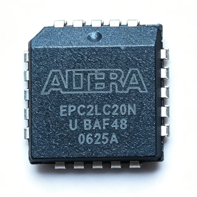
EPC2LC20N - 1.6Mb FPGA Configuration PROM, 20-PLCC | Intel
MPN: EPC2LC20N ✗ End of Life| Qty | Unit Price | Extended |
|---|---|---|
| 1 | $12.5 | $12.50 |
| 10 | $11.25 | $112.50 |
| 100 | $9.8 | $980.00 |
| 500 | $8.65 | $4,325.00 |
| 1,000 | $7.4 | $7,400.00 |
EPC2LC20N Overview
A configuration PROM (Programmable Read-Only Memory) is a non-volatile serial memory device whose sole purpose is to store the bitstream for an SRAM-based programmable logic device. Because SRAM-LUT FPGAs are volatile, their configuration must be reloaded on every power-up or reconfiguration event; the EPC2 family performs that role in a single-chip solution, replacing discrete EPROMs, microcontrollers, or boot-PROM arrangements. EPC2 devices sit in the boot-source hierarchy beneath FPGAs (CPLD -> glue logic -> PROM -> FPGA) and are an integral part of the Altera/Intel FPGA power-on sequencing ecosystem.
Key features of the EPC2LC20N include 1.6 Mbit of Flash storage, in-system programmability via JTAG, a built-in 8 MHz internal oscillator, and support for both 3.3 V and 5 V supply rails. It also provides a dedicated nSTATUS, nCONFIG, and CONF_DONE handshake to the target FPGA, eliminating the need for external glue logic in most designs.
The EPC2LC20N uses a 4-pin serial interface (DATA0, DCLK, nCONFIG, nSTATUS) to cascade-multiple PROMs can be chained to support larger FPGAs. The device supports FPGAs from the Altera APEX, Cyclone, Stratix, ACEX, and MAX 7000 families, with automatic baud-rate detection between the PROM and target device.
Typical applications include Altera/Intel Cyclone and APEX prototype boards, industrial control logic, telecom base-station FPGA boot cards, military/aerospace FPGA subsystems, and any system requiring multi-configuration support. The in-system programmability allows field upgrades without removing the PROM from the board.
When designing with this device, ensure proper decoupling (0.1 uF + 10 uF) on both VCC rails and respect the JTAG chain order if multiple PROMs are cascaded. The 5 V rail tolerance simplifies designs that mix 3.3 V FPGA I/O with 5 V configuration memory logic.
This page synthesizes distributor stock levels, drop-in Altera/Intel PROM alternatives, and JTAG-chain design notes not found on the original manufacturer datasheet.
Drop-in alternatives for EPC2LC20N — same package, pin-to-pin compatible. Different-package parts requiring PCB rework are excluded.
Variants in this series
Same-series models that are drop-in compatible with EPC2LC20N (same form factor and footprint) — differing in Memory Type, Package, Configuration Interface, Supported FPGA Families, Mounting Type.
Quick Comparison Tool — Select alternative parts for side-by-side comparison:
EPC2LI20N
✓ In Stock
$5.1 / Unit
View Datasheet →EPC2CC20N
✓ In Stock
$10.85 / Unit
View Datasheet →EPC2LC02N
✓ In Stock
$3.4 / Unit
View Datasheet →EPC2L20N
✓ In Stock
$17.2 / Unit
View Datasheet →EPC2LC8N
📋 Reference alternative (not in catalog)
EPC2LC40N
📋 Reference alternative (not in catalog)
EPC2LC20N Maximum Ratings & Electrical Characteristics
| Function | In-System Programmable Configuration PROM for SRAM-based FPGAs |
| Memory Size | 1.6 Mbit |
| Memory Type | Flash |
| Programmable Type | In System Programmable (ISP) |
| Supply Voltage VCCINT | 3.0 V to 3.6 V |
| Supply Voltage VCCIO | 4.75 V to 5.25 V |
| Configuration Clock Frequency | 8 MHz (max) |
| Interface | Serial (DATA0, DCLK, nCONFIG, nSTATUS, CONF_DONE) |
| JTAG Support | IEEE 1149.1 / IEEE 1532 compliant |
| Package | 20-pin PLCC (J-Lead, 9x9 mm) |
| Mounting Type | Surface Mount |
| Packaging | Tube |
| Supported FPGA Families | Altera APEX, Cyclone, Stratix, ACEX, MAX 7000 |
EPC2LC20N Pin Configuration
| Pin 1 | DATA0 — Configuration data output to target FPGA |
| Pin 2 | DCLK — Configuration clock input/output |
| Pin 3 | nCONFIG — Configuration control input (active low) |
| Pin 4 | nSTATUS — Configuration status output (active low) |
| Pin 5 | CONF_DONE — Configuration complete output |
| Pin 6 | TCK — JTAG test clock |
| Pin 7 | TMS — JTAG test mode select |
| Pin 8 | TDI — JTAG test data input |
| Pin 9 | TDO — JTAG test data output |
| Pin 10 | VCCINT — 3.3 V core supply (3.0 V to 3.6 V) |
| Pin 11 | GND — Ground |
| Pin 12 | VCCIO — 5 V I/O supply (4.75 V to 5.25 V) |
| Pin 13 | OE — Output enable (active low) |
| Pin 14 | CE — Chip enable (active low) |
| Pin 15 | MODE — Configuration mode select |
| Pin 16 | RESET — Reset input |
| Pin 17 | NC — Not connected (per datasheet) |
| Pin 18 | NC — Not connected (per datasheet) |
| Pin 19 | NC — Not connected (per datasheet) |
| Pin 20 | NC — Not connected (per datasheet) |
Typical Applications
EPC2LC20N is suitable for 7 applications: Altera Cyclone FPGA Boot Card, APEX / ACEX FPGA Configuration Source, Stratix Multi-Configuration Storage, Industrial PLC and Motion Controller, Telecom Base-Station FPGA Subsystem, Legacy 5V Military/Aerospace Subsystems, Test & Measurement Instrument Front End.
Altera Cyclone FPGA Boot Card
The EPC2LC20N's 1.6 Mbit Flash density is sized to match small-to-mid Altera Cyclone FPGA bitstreams (EP1C3, EP1C6, EP1C12 family), making it the canonical boot PROM for Cyclone-based industrial control and telecom cards. The 8 MHz internal oscillator and built-in nCONFIG/nSTATUS handshakes eliminate external glue logic, while the JTAG-ISP port lets engineers re-flash the bitstream in-field via Altera/Intel Quartus Programmer without removing the PROM. Operates from 3.0-3.6 V VCCINT and 4.75-5.25 V VCCIO, so it bridges legacy 5 V support circuitry with 3.3 V FPGA I/O on the same PCB.
Recommended
APEX / ACEX FPGA Configuration Source
Older Altera APEX 20K and ACEX 1K FPGAs rely on a 1.6 Mbit-class PROM, and the EPC2LC20N fits the bitstream sizes of EP20K60, EP20K100, and EP1K100 devices. The 4-pin serial interface (DATA0, DCLK, nCONFIG, nSTATUS) supports the Altera Passive Serial (PS) configuration scheme, allowing up to eight EPC2 PROMs to be cascaded in series for larger devices. The PLCC-20 J-lead package provides a robust through-hole-compatible footprint useful for legacy 5 V industrial systems that still use APEX or ACEX FPGAs.
Recommended
Stratix Multi-Configuration Storage
The EPC2LC20N stores one Stratix-class configuration image (up to 1.6 Mbit) and supports Altera's MultiBoot feature when cascaded with other EPC2 PROMs. Engineers building Stratix-based prototypes that need two configuration images (golden + update) can daisy-chain two EPC2LC20N devices: the FPGA selects between them via nCONFIG pulses at runtime. The JTAG-ISP port supports in-system re-flash of either PROM image without removing the card, simplifying field upgrades for telecom and military-aerospace subsystems.
Recommended
Industrial PLC and Motion Controller
PLC, motion controller, and CNC boards using Altera MAX 7000 or Cyclone FPGAs need a rugged configuration source. The EPC2LC20N's PLCC-20 socket compatibility allows it to be field-replaceable in legacy PLCs, and the JTAG-ISP interface lets technicians update firmware without desoldering. The 8 MHz configuration clock limits boot time to roughly 200 ms for a 1.6 Mbit image, fast enough for industrial power-on sequencing requirements. Engineers often pair the EPC2LC20N with watchdog supervisors for failsafe industrial boot.
Recommended
Telecom Base-Station FPGA Subsystem
Telecom base-station cards based on Altera APEX, Cyclone, or Stratix FPGAs use the EPC2LC20N to store the radio configuration bitstream and DSP firmware. The dual-rail supply (3.0-3.6 V and 4.75-5.25 V) supports mixed-voltage backplanes, while JTAG-ISP enables remote firmware push via boundary-scan test access ports. Cascade multiple EPC2LC20N devices for Stratix-class bitstreams that exceed 1.6 Mbit. The PLCC-20 socketed variant simplifies card-swap repairs in central-office environments.
Recommended
Legacy 5V Military/Aerospace Subsystems
The EPC2LC20N's 4.75-5.25 V VCCIO tolerance makes it one of the few configuration PROMs that drop into legacy 5 V military and aerospace subsystems that still use APEX or ACEX FPGAs. The PLCC-20 J-lead package withstands shock and vibration better than QFN equivalents, and the JTAG-ISP port supports the IEEE 1149.1 boundary-scan testing required by many defense programs. Engineers can re-flash the bitstream in-system via JTAG, eliminating the need for socketed EPROMs on the production board.
Recommended
Test & Measurement Instrument Front End
Test instruments (oscilloscopes, logic analyzers, signal generators) built on Altera Cyclone or Stratix FPGAs use the EPC2LC20N as a rugged boot PROM. The JTAG-ISP port supports field firmware updates as new measurement algorithms are released, and the 8 MHz internal oscillator guarantees deterministic boot time across temperature. The PLCC-20 socketed option simplifies factory rework on test-and-measurement production lines that frequently swap bitstreams for different SKUs.
Recommended
Recommended Products Summary
Engineering reference data for EPC2LC20N — comparison, design guidance, and compliance information.
Selection Guide
Comparison with Alternatives
| Parameter | This Product | EPC2LI20N | EPC2LC8N | EPC2LC40N | EPC2CC20N | EPC2L20N |
|---|---|---|---|---|---|---|
| Package | 20-PLCC (J-Lead, 9x9) | 20-PLCC (J-Lead, 9x9) - same | 20-PLCC (J-Lead, 9x9) - same | 20-PLCC (J-Lead, 9x9) - same | 20-PLCC (J-Lead, 9x9) - same | 20-PLCC (J-Lead, 9x9) - same |
| Brand | Intel | Intel - same | Intel - same | Intel - same | Intel - same | Intel - same |
| Memory Size | 1.6 Mbit | 1.6 Mbit | 0.8 Mbit (-50%) | 4 Mbit (+150%) | 1.6 Mbit | 1.6 Mbit |
| Supply Voltage VCCINT | 3.0 V to 3.6 V | 3.0 V to 3.6 V | 3.0 V to 3.6 V | 3.0 V to 3.6 V | 3.0 V to 3.6 V | 3.0 V to 3.6 V |
| Supply Voltage VCCIO | 4.75 V to 5.25 V | 4.75 V to 5.25 V | 4.75 V to 5.25 V | 4.75 V to 5.25 V | 4.75 V to 5.25 V | 4.75 V to 5.25 V |
| Configuration Clock | 8 MHz | 8 MHz | 8 MHz | 8 MHz | 8 MHz | 8 MHz |
| JTAG-ISP | Yes (IEEE 1149.1) | Yes (IEEE 1149.1) | Yes (IEEE 1149.1) | Yes (IEEE 1149.1) | Yes (IEEE 1149.1) | Yes (IEEE 1149.1) |
| Operating Temperature | Commercial (0C to +70C) | Industrial (-40C to +85C) | Commercial (0C to +70C) | Commercial (0C to +70C) | Commercial (0C to +70C) | Commercial (0C to +70C) |
| Lifecycle Status | NRND | NRND | NRND | NRND | NRND | NRND |
Key Differentiators
- Dual-rail supply (3.3 V + 5 V) supports legacy 5 V systems (vs EPC2LI20N)
- 1.6 Mbit density matches Cyclone-class bitstreams exactly (vs EPC2LC8N)
- Single-chip alternative to discrete EPROMs or MCU boot-loaders (vs EPC2LC40N)
Design Notes
The EPC2LC20N requires two supplies: VCCINT at 3.0 V to 3.6 V (typical 3.3 V) and VCCIO at 4.75 V to 5.25 V (typical 5.0 V). Place a 0.1 uF ceramic decoupling capacitor within 5 mm of each VCC pin, with a 10 uF bulk capacitor on each rail near the IC. Power-up sequencing requires VCCIO to rise no later than VCCINT; if sequencing cannot be guaranteed, add a Schottky diode between VCCIO and VCCINT to prevent latch-up. Estimated: typical ICCINT = 25 mA, ICCIO = 15 mA during configuration (verify on datasheet).
Route the 4-pin serial configuration bus (DATA0, DCLK, nCONFIG, nSTATUS) as short, impedance-matched traces (target 50 ohm) and keep them at least 3 mm away from switching-power or high-speed RF traces. The JTAG chain (TCK, TMS, TDI, TDO) should also be routed short and length-matched if multiple devices share the chain. Place a 10 kohm pull-up on nCONFIG and a 10 kohm pull-up on nSTATUS to VCCIO. Add a 1 kohm series resistor on TDO to damp reflections if the JTAG chain exceeds 100 mm.
Critical pitfalls when designing with the EPC2LC20N: (1) Do not exceed 5.25 V on VCCIO - the PLCC-20 EPC2 family is not 5 V-tolerant above this. (2) Do not cascade more than 8 EPC2 PROMs in series - the nCONFIG/nSTATUS handshakes become unreliable beyond this count. (3) When migrating to EPCQ-series PROMs, note that the EPCQ uses a different configuration-mode pinout - PCB redesign is required. (4) Do not assume the PROM auto-detects the FPGA family - verify configuration-mode selection via the MODE pin. (5) Always run the Quartus Programmer 'Blank-Check + Verify' after ISP to confirm bitstream integrity.
Place the EPC2LC20N PLCC-20 socket within 50 mm of the target FPGA's configuration pins to minimize trace capacitance. Keep the JTAG connector within 25 mm of the PROM's TDI/TDO/TCK/TMS pins, with a 4.7 kohm pull-up on TCK and TMS to prevent spurious JTAG state transitions during power-up. Use a ground guard trace around the DCLK line to reduce crosstalk into DATA0. If the design supports in-system re-flash via JTAG, expose the JTAG pins on a 0.1 inch header for production programming access.
Compliance Information
RoHS/REACH status not explicitly stated in the verified web data or datasheet extract provided. EPC2 family uses PLCC-20 J-lead package; many legacy Altera PLCC parts are non-RoHS. Verify on the Intel/Avnet distributor product page before designing into a RoHS-only BOM.



