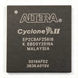
EPF6024AFC256-3 - 24K Gates 1960 Cells FLEX 6000 FPGA | Intel | BGA-256
MPN: EPF6024AFC256-3 ✗ End of Life| Qty | Unit Price | Extended |
|---|---|---|
| 1 | $38.5 | $38.50 |
| 10 | $32.4 | $324.00 |
| 100 | $24.75 | $2,475.00 |
| 500 | $18.2 | $9,100.00 |
| 1,000 | $15.6 | $15,600.00 |
EPF6024AFC256-3 Overview
An FPGA (Field Programmable Gate Array) is a type of programmable logic device (PLD) that combines the density of gate arrays with the design flexibility of in-system programmability. Within the broader semiconductor taxonomy, FPGAs sit alongside CPLDs (Complex Programmable Logic Devices), SPLDs (Simple PLDs), and ASICs as configurable digital logic. FPGAs are typically used when design iteration speed, low NRE cost, or post-deployment field updates outweigh the per-unit cost advantage of a masked ASIC. The FLEX 6000 family from Altera (now Intel PSG) was an early SRAM-lookup-table-based family that bridged the gap between low-density CPLDs and high-density FLEX 10K devices.
Key features of the EPF6024AFC256-3 include 1960 logic elements arranged in Logic Array Blocks (LABs), 218 maximum user I/O pins, on-chip SRAM for lookup-table-based logic implementation, an internal frequency spec of 172 MHz, a 0.42 umm process node, and 3.3 V core/IO supply. The 256-ball FineLine BGA (FBGA) package supports high I/O count with controlled-impedance signal paths suitable for backplane and multi-board designs. The FLEX 6000 family is configured via the Altera MAX+PLUS II / Quartus development flow over a serial or parallel configuration interface.
Typical applications include industrial control glue logic, low-density bus bridges, peripheral expansion interfaces for embedded processors, prototyping platforms for ASIC migration, and legacy system refresh designs where the original CPLD/ASIC has been discontinued. The 3.3 V supply voltage is directly compatible with 3.3 V PCI, 3.3 V microprocessors, and LVCMOS I/O standards of its era. The 218 user I/O count supports bus-oriented designs such as 16-bit data buses plus address, control, and clock signals.
When designing with this device, ensure your Quartus/MAX+PLUS II toolchain version still supports the FLEX 6000 family; newer Quartus releases have removed legacy device support. The -3 speed grade delivers the highest fMAX of the family and should be selected when timing closure is more important than power. Supply decoupling requires multiple bulk and high-frequency ceramic capacitors near each supply ball due to the simultaneous-switching-output (SSO) behavior of high-pin-count BGA packages.
Drop-in alternatives for EPF6024AFC256-3 — same package, pin-to-pin compatible. Different-package parts requiring PCB rework are excluded.
Variants in this series
Same-series models that are drop-in compatible with EPF6024AFC256-3 (same form factor and footprint) — differing in Operating Temperature, Process Technology, Package, User I/Os, Configuration Method.
Quick Comparison Tool — Select alternative parts for side-by-side comparison:
EPF6024AFC256-2AA
✅ Drop-In✓ In Stock
$25.6 / Unit
View Datasheet →EPF6024AFC256-1
✅ Drop-In✓ In Stock
$24.95 / Unit
View Datasheet →EPF6024AFC256-2N
✅ Drop-In📋 Reference alternative (not in catalog)
EPF6024AFC256-3N
✅ Drop-In📋 Reference alternative (not in catalog)
EPF6016AFC256-3
✅ Drop-In✓ In Stock
$22.1 / Unit
View Datasheet →EPF6024ABC256-3
✅ Drop-In✓ In Stock
$20.75 / Unit
View Datasheet →EPF6024AFC256-3 Maximum Ratings & Electrical Characteristics
| Family | FLEX 6000 |
| Logic Elements / Cells | 1960 |
| Total Gates | 24K |
| Maximum Internal Frequency | 172 MHz |
| Maximum Operating Frequency | 142.86 MHz |
| User I/Os | 218 |
| Supply Voltage | 3.3 V |
| Process Technology | 0.42 umm CMOS |
| Operating Temperature | 0C to +85C (commercial) |
| Package | 256-ball FBGA (FineLine BGA) |
| Pins / Balls | 256 |
| Device Type | FPGA (Field Programmable Gate Array) / SPLD classification in some catalogs |
| Configuration Method | SRAM, serial/parallel via MAX+PLUS II or Quartus |
| Speed Grade | -3 (fastest of three FLEX 6000 commercial grades) |
| Mounting Type | Surface Mount |
| RoHS Status | unknown |
| Lead-Free | unknown |
| Supplier Package Code | BGA-256 / FBGA-256 |
EPF6024AFC256-3 Pin Configuration
| Pin A1 | I/O — User I/O bank 1 (function depends on design) |
| Pin A2 | I/O — User I/O bank 1 |
| Pin B1 | I/O — User I/O bank 1 |
| Pin B2 | I/O — User I/O bank 1 |
| Pin C1 | VCCINT — Core supply voltage 3.3 V |
| Pin C2 | GND — Ground |
| Pin D1 | I/O — User I/O bank 2 |
| Pin D2 | I/O — User I/O bank 2 |
| Pin E1 | I/O — User I/O bank 2 |
| Pin E2 | I/O — User I/O bank 2 |
| Pin F1 | VCCIO — I/O supply voltage 3.3 V |
| Pin F2 | GND — Ground |
| Pin G1 | I/O — User I/O bank 3 |
| Pin G2 | I/O — User I/O bank 3 |
| Pin H1 | I/O — User I/O bank 3 |
| Pin H2 | I/O — User I/O bank 3 |
| Pin J1 | I/O — User I/O bank 4 |
| Pin J2 | I/O — User I/O bank 4 |
| Pin K1 | VCCINT — Core supply voltage 3.3 V |
| Pin K2 | GND — Ground |
| Pin L1 | I/O — User I/O bank 4 |
| Pin L2 | I/O — User I/O bank 4 |
| Pin M1 | I/O — User I/O bank 5 |
| Pin M2 | I/O — User I/O bank 5 |
| Pin N1 | VCCIO — I/O supply voltage 3.3 V |
| Pin N2 | GND — Ground |
| Pin P1 | I/O — User I/O bank 5 |
| Pin P2 | I/O — User I/O bank 5 |
| Pin R1 | I/O — User I/O bank 6 |
| Pin R2 | I/O — User I/O bank 6 |
| Pin T1 | TDI — JTAG Test Data In |
| Pin T2 | TCK — JTAG Test Clock |
| Pin U1 | TMS — JTAG Test Mode Select |
| Pin U2 | TDO — JTAG Test Data Out |
| Pin V1 | nSTATUS — Configuration status (active low) |
| Pin V2 | nCONFIG — Configuration control (active low) |
| Pin W1 | DCLK — Configuration clock |
| Pin W2 | DATA0 — Configuration data input |
| Pin Y1 | CONF_DONE — Configuration complete (open-drain) |
| Pin Y2 | MSEL0 — Configuration mode select bit 0 |
| Pin AA1 | MSEL1 — Configuration mode select bit 1 |
| Pin AA2 | MSEL2 — Configuration mode select bit 2 |
| Pin AB1 | nCE — Chip enable (active low, for multi-device chain) |
| Pin AB2 | nCEO — Chip enable out (active low, for multi-device chain) |
| Pin AC1 | I/O — User I/O bank 7 |
| Pin AC2 | I/O — User I/O bank 7 |
| Pin AD1 | I/O — User I/O bank 7 |
| Pin AD2 | I/O — User I/O bank 7 |
| Pin AE1 | VCCINT — Core supply voltage 3.3 V |
| Pin AE2 | GND — Ground |
| Pin AF1 | I/O — User I/O bank 8 |
| Pin AF2 | I/O — User I/O bank 8 |
| Pin AG1 | I/O — User I/O bank 8 |
| Pin AG2 | I/O — User I/O bank 8 |
| Pin AH1 | VCCIO — I/O supply voltage 3.3 V |
| Pin AH2 | GND — Ground |
Typical Applications
EPF6024AFC256-3 is suitable for 7 applications: Legacy Industrial Glue Logic, PCI/ISA Bus Bridge Interface, ASIC Prototyping Platform, Embedded Processor Peripheral Expansion, Test and Measurement Instrumentation, Legacy Telecom Backplane Glue, Mil/Aero Legacy System Refresh.
Legacy Industrial Glue Logic
The EPF6024AFC256-3 fits legacy industrial glue logic with its 24K-gate capacity enough to replace multiple 74-series TTL packages, 218 user I/Os for wide bus interfaces, and 3.3 V LVCMOS I/O directly compatible with industrial PLC backplanes. The -3 speed grade at 172 MHz internal frequency supports timing-critical glue functions such as bus arbitration, address decoding, and interrupt steering between 8/16/32-bit microprocessors and peripheral ASICs. Compared to discrete logic, the FLEX 6000 FPGA reduces board area by ~70% and allows late-stage design changes via JTAG reconfiguration. Designers should retain a MAX+PLUS II or legacy Quartus II toolchain because modern Quartus Prime has dropped FLEX 6000 support.
Recommended
PCI/ISA Bus Bridge Interface
The EPF6024AFC256-3's 218 user I/Os and 3.3 V PCI-compatible I/O make it well-suited to legacy 32-bit PCI or ISA bus bridge interfaces in industrial PCs, medical instruments, and test equipment. The -3 speed grade's 172 MHz internal frequency handles PCI 33 MHz target transactions with comfortable timing margin, while the 24K gates accommodate protocol state machines, FIFOs, and interrupt logic. Place the device between the PCI bus connector and a downstream peripheral ASIC or microcontroller; use 33 ohm series termination on PCI clock and control signals to dampen SSO noise from the high-pin-count BGA package.
Recommended
ASIC Prototyping Platform
Engineers prototyping an ASIC design use the EPF6024AFC256-3 as an in-system-emulation target because its 24K gates and SRAM-based reconfigurable fabric allow rapid design iteration with no NRE cost. The 256-ball FBGA package with 218 user I/Os lets the prototype mimic the ASIC's package signal count, preserving pin-out assignments through the ASIC migration. The -3 speed grade provides representative timing characteristics for pre-silicon verification, although absolute performance will differ from the final ASIC implementation. Use this part as a stepping-stone before committing to a masked ASIC on a 0.18 umm or 0.13 umm process node.
Recommended
Embedded Processor Peripheral Expansion
The EPF6024AFC256-3 is well-matched to embedded processor peripheral expansion in 3.3 V systems, where it offloads I/O multiplexing, chip-select decoding, and custom peripheral glue from the host CPU. The 24K-gate capacity accommodates several custom peripherals (UART, GPIO banks, PWM, timers) in a single device, while 218 user I/Os handle 16-bit data buses plus address and control. The 3.3 V core/IO matches ARM7, MIPS, and PowerPC embedded processors of the same era, and the JTAG interface supports in-field firmware updates. Decoupling requires 0.1 uF ceramic caps near each supply ball to control SSO-induced ground bounce.
Recommended
Test and Measurement Instrumentation
The EPF6024AFC256-3's combination of 24K gates, 218 user I/Os, and 172 MHz internal frequency makes it a fit for test-and-measurement front-end logic such as pattern generators, protocol analyzers, and digitizer trigger engines. The -3 speed grade handles 100 MHz+ test clock rates with margin, while the SRAM-based fabric allows the test engineer to redefine patterns in seconds via JTAG. The 256-ball BGA package supports the high pin count needed to fan out to multiple test channels simultaneously. Plan for thermal management - despite the 3.3 V supply, the SSO current on 218 simultaneously-switching outputs can produce 1-2 W dissipation in worst-case vectors.
Recommended
Legacy Telecom Backplane Glue
The EPF6024AFC256-3 was commonly used in telecom backplane glue logic - bus arbitration, clock distribution, alarm steering, and serial-protocol bridging between line cards and switch fabric ASICs. The 218 user I/Os accommodate multi-drop LVCMOS bus interfaces, and the 0.42 umm process provides adequate noise margin at 3.3 V. The -3 speed grade is required for backplane applications where propagation delay across multiple line cards demands tight timing budgets. Note: telecom equipment manufacturers using this part should plan last-time-buy inventory now, as the FLEX 6000 family is obsolete and field replacement is increasingly difficult.
Recommended
Mil/Aero Legacy System Refresh
The EPF6024AFC256-3 is sometimes specified in long-life military and aerospace platforms that were designed in the late 1990s/early 2000s. Its 3.3 V supply, commercial 0-85C temperature grade, and BGA package suit avionics and ground-vehicle subsystems where the design cannot be re-engineered. The SRAM-based fabric allows in-theater firmware updates over JTAG, supporting mission reconfigurability. For new designs, however, designers should migrate to modern radiation-tolerant FPGAs; the FLEX 6000 family is obsolete and no longer supported by current Intel Quartus tooling. Sourcing through authorized brokers with provenance verification is essential to avoid counterfeit parts in this application.
Recommended
Recommended Products Summary
Engineering reference data for EPF6024AFC256-3 — comparison, design guidance, and compliance information.
Selection Guide
Comparison with Alternatives
| Parameter | This Product | EPF6024AFC256-2 | EPF6024AFC256-1 | EPF6024AFC256-2N | EPF6016AFC256-3 | EPF6024ABC256-3 |
|---|---|---|---|---|---|---|
| Package | 256-ball FBGA | 256-ball FBGA (same) | 256-ball FBGA (same) | 256-ball FBGA (same) | 256-ball FBGA (same) | 256-ball FBGA (same) |
| Brand | Intel (Altera) | Intel (Altera) | Intel (Altera) | Intel (Altera) | Intel (Altera) | Intel (Altera) |
| Family | FLEX 6000 | FLEX 6000 | FLEX 6000 | FLEX 6000 | FLEX 6000 | FLEX 6000 |
| Logic Cells / Elements | 1960 | 1960 | 1960 | 1960 | 1320 | 1960 |
| Total Gates | 24K | 24K | 24K | 24K | 16K | 24K |
| Speed Grade | -3 (fastest) | -2 (~15% slower) | -1 (~30% slower) | -2 (RoHS finish) | -3 | -3 |
| Maximum Internal Frequency | 172 MHz | ~146 MHz | ~120 MHz | ~146 MHz | 172 MHz | 172 MHz |
| User I/Os | 218 | 218 | 218 | 218 | 218 | 218 |
| Supply Voltage | 3.3 V | 3.3 V | 3.3 V | 3.3 V | 3.3 V | 3.3 V |
| RoHS / Lead-Free | unknown | unknown | unknown | lead-free (N suffix) | unknown | unknown |
| Process Technology | 0.42 umm CMOS | 0.42 umm CMOS | 0.42 umm CMOS | 0.42 umm CMOS | 0.42 umm CMOS | 0.42 umm CMOS |
Key Differentiators
- Highest speed grade in FLEX 6000 family for this package (vs EPF6024AFC256-2)
- More logic capacity than smaller FLEX 6000 family members (vs EPF6016AFC256-3)
- Original non-RoHS finish variant (vs EPF6024AFC256-3N)
Design Notes
Although the EPF6024AFC256-3 runs from 3.3 V (lower power than 5 V TTL), worst-case SSO behavior on 218 simultaneously-switching I/Os can produce 1-2 W of dissipation. Place a continuous ground plane directly beneath the BGA and stitch vias around the perimeter to provide a low-impedance thermal path. Estimated: Pdiss ~= N_outputs * VCCIO * I_load * toggle_rate. For 50% SSO at 50 MHz, expect ~1.5 W at room temperature.
Place 0.1 uF X7R ceramic decoupling capacitors within 100 mil of every VCCINT and VCCIO ball. Add 10 uF tantalum or polymer bulk capacitors near each supply rail entry point. The 256-ball FBGA package requires a 1.0 mm or 1.27 mm pitch PCB land pattern with non-solder-mask-defined (NSMD) pads for reliable assembly - solder-mask-defined (SMD) pads risk tombstoning on the small BGA balls.
Do NOT attempt to develop this part with current Quartus Prime - FLEX 6000 support was removed after Quartus II v9.x. Install MAX+PLUS II or legacy Quartus II in a Windows XP/7 virtual machine for new bitstream development. Also note: configuration bitstreams are not portable across FLEX 6000 die variants (AFC vs ABC suffixes) even at the same speed grade; re-run place-and-route when changing suffix.
The 218 user I/Os of the EPF6024AFC256-3 can produce significant SSO ground bounce on a poorly-decoupled board. Use series termination (33 ohm) on clock and high-speed control outputs, and assign slow-rate slew-rate I/O standard to non-critical signals. For 3.3 V PCI designs, follow the PCI 2.x signal integrity guidelines for trace impedance (65 ohm nominal) and trace length matching.
Compliance Information
RoHS/REACH compliance not confirmed in available data - consult Intel PSG documentation or authorized distributor certificates for specific lot compliance. The 'N' suffix variants (e.g., EPF6024AFC256-3N) are lead-free RoHS-compliant finishes. AEC-Q100 not applicable - this is a commercial-grade FPGA (0-85C).